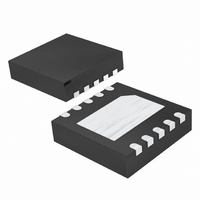
MAX1396ETB+T Maxim Integrated Products, MAX1396ETB+T Datasheet - Page 4

MAX1396ETB+T
Manufacturer Part Number
MAX1396ETB+T
Description
IC ADC 12BIT 312.5KSPS 10-TDFN
Manufacturer
Maxim Integrated Products
Datasheet
1.MAX1396ETBT.pdf
(18 pages)
Specifications of MAX1396ETB+T
Number Of Bits
12
Sampling Rate (per Second)
312.5k
Data Interface
DSP, MICROWIRE™, QSPI™, Serial, SPI™
Number Of Converters
1
Power Dissipation (max)
830µW
Voltage Supply Source
Single Supply
Operating Temperature
-40°C ~ 85°C
Mounting Type
Surface Mount
Package / Case
10-WFDFN Exposed Pad
Number Of Adc Inputs
2
Architecture
SAR
Conversion Rate
312 KSPs
Resolution
12 bit
Interface Type
Serial
Voltage Reference
External
Supply Voltage (max)
3.3 V
Mounting Style
SMD/SMT
Lead Free Status / RoHS Status
Lead free / RoHS Compliant
Other names
MAX1396ETB+T
1.5V to 3.6V, 312.5ksps, 1-Channel True-Differential/
2-Channel Single-Ended, 12-Bit, SAR ADCs
TIMING CHARACTERISTICS
(V
T
ELECTRICAL CHARACTERISTICS (continued)
(V
T
4
Note 1: V
Note 2: V
Note 3: All digital inputs swing between V
Note 4: CS = V
Note 5: CS = V
Note 6: Change in V
Tri-State Leakage Current
Tri-State Output Capacitance
POWER SUPPLY
Positive Supply Voltage
Positive Supply Current (Note 3)
Power-Supply Rejection
A
A
SCLK Clock Period
SCLK Pulse-Width High
SCLK Pulse-Width Low
CS Fall to SCLK Rise Setup
SCLK Rise to CS Fall Ignore
SCLK Fall to DOUT Valid
OE Rise to DOUT Disable
OE Fall to DOUT Enable
CS Pulse-Width High or Low
OE Pulse-Width High or Low
CH1/CH2 Setup Time (to the
First SCLK)
CH1/CH2 Hold Time (to the First
SCLK)
UNI/BIP Setup Time (to the First
SCLK)
UNI/BIP Hold Time (to the First
SCLK)
DD
DD
= +25°C.) (Figure 1)
= +25°C.)
_______________________________________________________________________________________
= +1.5V to +3.6V, V
= +1.5V to +3.6V, V
DD
DD
PARAMETER
PARAMETER
= 1.5V, V
= 1.5V, V
DD
DD
, OE = UNI/BIP = CH1/CH2 = V
, OE = UNI/BIP = CH1/CH2 = V
AIN
REF
REF
at code boundary 4094.5.
REF
REF
= 1.5V, and V
= 1.5V, V
= V
= V
DD
DD
, C
AIN
, C
SYMBOL
SYMBOL
REF
REF
C
t
t
t
t
t
t
t
t
t
= 1.5V
t
t
V
PSR
DOD
CSW
OEW
I
t
CSO
DOV
DOE
CHS
CHH
UBH
AIN
t
t
CSS
UBS
I
OUT
DD
CH
CP
CL
LT
DD
DD
= 0.1μF, f
= 0.1μF, f
= 1.5V.
and GND. V
P-P
, f
OE = V
OE = V
f
f
Power-down mode (Note 4)
Power-down mode (Note 5)
V
DD
DD
SAMPLE
SAMPLE
C
MAX1396 only
MAX1396 only
MAX1393 only
MAX1393 only
DD
SCLK
LOAD
SCLK
SCLK
or GND, SCLK is active.
or GND, SCLK is inactive.
= 1.5V to 3.6V, full-scale input (Note 6)
DD
DD
= 5MHz, f
REF
= 0 to 30pF
= 100ksps
= 312.5ksps
= 5MHz, T
= 5MHz, T
= V
DD
CONDITIONS
CONDITIONS
SAMPLE
, f
IN
A
A
= T
= T
= 75kHz sine wave, V
MIN
MIN
= 312.5ksps, and f
to T
to T
V
V
V
V
DD
DD
DD
DD
MAX
MAX
= 1.6V
= 3V
= 1.6V
= 3V
, unless otherwise noted. Typical values are at
, unless otherwise noted. Typical values are at
AIN
IN
(sine wave) = 75kHz.
= V
MIN
MIN
200
1.5
90
90
80
10
80
80
10
10
0
0
0
REFP-P,
±150
TYP
TYP
C
176
225
520
710
0.2
10
6
9
5
LOAD
= 30pF on DOUT.
10,000
±1000
MAX
MAX
±2.5
200
260
600
800
3.6
±1
10
80
20
20
UNITS
UNITS
μV/V
μA
pF
μA
ns
ns
ns
ns
ns
ns
ns
ns
ns
ns
ns
ns
ns
ns
V


