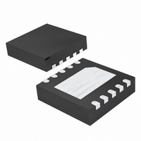
MAX1396ETB+T Maxim Integrated Products, MAX1396ETB+T Datasheet - Page 13

MAX1396ETB+T
Manufacturer Part Number
MAX1396ETB+T
Description
IC ADC 12BIT 312.5KSPS 10-TDFN
Manufacturer
Maxim Integrated Products
Datasheet
1.MAX1396ETBT.pdf
(18 pages)
Specifications of MAX1396ETB+T
Number Of Bits
12
Sampling Rate (per Second)
312.5k
Data Interface
DSP, MICROWIRE™, QSPI™, Serial, SPI™
Number Of Converters
1
Power Dissipation (max)
830µW
Voltage Supply Source
Single Supply
Operating Temperature
-40°C ~ 85°C
Mounting Type
Surface Mount
Package / Case
10-WFDFN Exposed Pad
Number Of Adc Inputs
2
Architecture
SAR
Conversion Rate
312 KSPs
Resolution
12 bit
Interface Type
Serial
Voltage Reference
External
Supply Voltage (max)
3.3 V
Mounting Style
SMD/SMT
Lead Free Status / RoHS Status
Lead free / RoHS Compliant
Other names
MAX1396ETB+T
1.5V to 3.6V, 312.5ksps, 1-Channel True-Differential/
Figure 10. DSP Serial-Timing Diagram
As shown in Figure 11, drive the MAX1393/MAX1396
chip-select input (CS) with the DSP’s frame-sync signal.
OE may be connected to GND or driven independently.
For continuous conversion operation, keep OE low and
make the CS falling edge coincident with the 16th
falling edge of the SCLK.
Low operating voltage (1.5V to 3.6V) and ultra-low-power
consumption make the MAX1393/MAX1396 ideal for low
cost, unregulated, battery-powered applications without
the need for a DC-DC converter. Power the MAX1393/
MAX1396 directly from two alkaline/NiMH/NiCd cells in
series or a single lithium coin cell as shown in the Typical
Operating Circuit .
Fresh alkaline cells have a voltage of approximately
1.5V per cell (3V with 2 cells in series) and approach
end of life at 0.8V (1.6V with 2 cells in series). A typical
2xAA alkaline discharge curve is shown in Figure 12a.
A typical CR2032 lithium (LiMnO
curve is shown in Figure 12b.
For best performance, use PC boards. Board layout
must ensure that digital and analog signal lines are
separated from each other. Do not run analog and digi-
tal (especially clock) lines parallel to one another, or
digital lines underneath the ADC package.
(CH1/CH2)*
*INDICATES THE MAX1396
UNI/BIP
STATE
DOUT
SCLK
ADC
Unregulated Two-Cell or Single Lithium
CS
OE
POWER-
DOWN
Layout, Grounding, and Bypassing
D0
16
______________________________________________________________________________________
1
BIPOLAR (AIN1)*
2-Channel Single-Ended, 12-Bit, SAR ADCs
AND ACQUIRE
POWER-UP
(t
ACQ
2
)
LiMnO
3
2
) coin cell discharge
2
4
SAMPLING INSTANT
Cell Operation
D11
5
D10
6
D9
7
D8
8
Figure 13 shows the recommended system ground
connections. Establish a single-point analog ground
(star ground point) at the MAX1393/MAX1396s’ GND
pin or use the ground plane.
High-frequency noise in the power supply (V
degrades the ADC’s performance. Bypass V
with a 0.1μF capacitor as close to the device as possi-
ble. Minimize capacitor lead lengths for best supply
noise rejection. To reduce the effects of supply noise, a
10Ω resistor can be connected as a lowpass filter to
attenuate supply noise.
The MAX1393/MAX1396 TDFN package has an
exposed pad on the bottom of the package. This pad is
not internally connected. Connect the exposed pad to
the GND pin on the MAX1393/MAX1396 or leave
unconnected for proper electrical performance.
INL is the deviation of the values on an actual transfer
function from a straight line. For the MAX1393/
MAX1396, this straight line is between the end points of
the transfer function once offset and gain errors have
been nullified. INL deviations are measured at every
step and the worst-case deviation is reported in the
Electrical Characteristics section.
AND CONVERT
D7
9
(t
HOLD
CONV
)
10
D6
11
D5
12
D4
Integral Nonlinearity (INL)
13
D3
14
D2
15
D1
Definitions
Exposed Pad
FS
16
D0
POWER-
DOWN
UNI (AIN2)*
DD
1
to GND
2
DD
13
)


