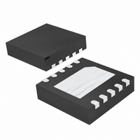
MAX1396ETB+T Maxim Integrated Products, MAX1396ETB+T Datasheet - Page 10

MAX1396ETB+T
Manufacturer Part Number
MAX1396ETB+T
Description
IC ADC 12BIT 312.5KSPS 10-TDFN
Manufacturer
Maxim Integrated Products
Datasheet
1.MAX1396ETBT.pdf
(18 pages)
Specifications of MAX1396ETB+T
Number Of Bits
12
Sampling Rate (per Second)
312.5k
Data Interface
DSP, MICROWIRE™, QSPI™, Serial, SPI™
Number Of Converters
1
Power Dissipation (max)
830µW
Voltage Supply Source
Single Supply
Operating Temperature
-40°C ~ 85°C
Mounting Type
Surface Mount
Package / Case
10-WFDFN Exposed Pad
Number Of Adc Inputs
2
Architecture
SAR
Conversion Rate
312 KSPs
Resolution
12 bit
Interface Type
Serial
Voltage Reference
External
Supply Voltage (max)
3.3 V
Mounting Style
SMD/SMT
Lead Free Status / RoHS Status
Lead free / RoHS Compliant
Other names
MAX1396ETB+T
1.5V to 3.6V, 312.5ksps, 1-Channel True-Differential/
2-Channel Single-Ended, 12-Bit, SAR ADCs
A falling edge on CS initiates the power-up sequence
and begins acquiring the analog input as long as OE is
also asserted low. On the 3rd SCLK falling edge, the
analog input is held for conversion. The most significant
bit (MSB) decision is made and clocked onto DOUT on
the 4th SCLK falling edge. Valid DOUT data is available
to be clocked into the master (microcontroller (μC)) on
the following SCLK rising edge. The rest of the bits are
decided and clocked out to DOUT on each successive
SCLK falling edge. See Figures 8 and 9 for conversion
timing diagrams.
Once a conversion has been initiated, CS can go high at
any time. Further falling edges of CS do not reinitiate an
acquisition cycle until the current conversion completes.
Once a conversion completes, the first falling edge of CS
begins another acquisition/conversion cycle.
Figure 5. Unipolar Transfer Function
10
______________________________________________________________________________________
FFD
FFC
FFB
FFF
FFE
004
003
002
001
000
0
1 LSB =
FS = V
1
ZS = 0
Applications Information
2
REF
4096
V
REF
3
INPUT VOLTAGE (LSB)
4
Starting a Conversion
FULL-SCALE
TRANSITION
FS - 1.5 LSB
FS
Drive UNI/BIP high to select unipolar mode or pull
UNI/BIP low to select bipolar mode. UNI/BIP can be
connected to V
or actively driven. UNI/BIP needs to be stable for t
prior to the first rising edge of SCLK after the CS falling
edge (see Figure 1) for a valid conversion result when
being actively driven.
Pull CH1/CH2 low to select AIN1 or drive CH1/CH2
high to select AIN2 for conversion. CH1/CH2 can be
connected to V
or actively driven. CH1/CH2 needs to be stable for t
prior to the first rising edge of SCLK after the CS falling
edge (see Figure 1) for a valid conversion result when
being actively driven.
Figure 6. Bipolar Transfer Function
7FF
7FE
001
000
FFF
FFE
801
800
Selecting Analog Input AIN1 or AIN2
Selecting Unipolar or Bipolar Mode
-FS
+FS = V
1 LSB =
ZS = 0
-FS =
DD
DD
-V
REF
2
2
REF
-FS + 0.5 LSB
4096
V
REF
for logic high, to GND for logic low,
for logic high, to GND for logic low,
INPUT VOLTAGE (LSB)
0
FULL-SCALE
TRANSITION
+FS - 1.5 LSB
(MAX1393 Only)
(MAX1396 Only)
+FS
CHS
UBS


