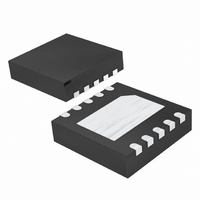
MAX1396ETB+T Maxim Integrated Products, MAX1396ETB+T Datasheet - Page 2

MAX1396ETB+T
Manufacturer Part Number
MAX1396ETB+T
Description
IC ADC 12BIT 312.5KSPS 10-TDFN
Manufacturer
Maxim Integrated Products
Datasheet
1.MAX1396ETBT.pdf
(18 pages)
Specifications of MAX1396ETB+T
Number Of Bits
12
Sampling Rate (per Second)
312.5k
Data Interface
DSP, MICROWIRE™, QSPI™, Serial, SPI™
Number Of Converters
1
Power Dissipation (max)
830µW
Voltage Supply Source
Single Supply
Operating Temperature
-40°C ~ 85°C
Mounting Type
Surface Mount
Package / Case
10-WFDFN Exposed Pad
Number Of Adc Inputs
2
Architecture
SAR
Conversion Rate
312 KSPs
Resolution
12 bit
Interface Type
Serial
Voltage Reference
External
Supply Voltage (max)
3.3 V
Mounting Style
SMD/SMT
Lead Free Status / RoHS Status
Lead free / RoHS Compliant
Other names
MAX1396ETB+T
1.5V to 3.6V, 312.5ksps, 1-Channel True-Differential/
2-Channel Single-Ended, 12-Bit, SAR ADCs
ABSOLUTE MAXIMUM RATINGS
V
SCLK, CS, OE, CH1/CH2, UNI/BIP,
AIN+, AIN-, AIN1, AIN2, REF to GND ........-0.3V to (V
Maximum Current into Any Pin .........................................±50mA
Continuous Power Dissipation (T
ELECTRICAL CHARACTERISTICS
(V
T
Stresses beyond those listed under “Absolute Maximum Ratings” may cause permanent damage to the device. These are stress ratings only, and functional
operation of the device at these or any other conditions beyond those indicated in the operational sections of the specifications is not implied. Exposure to
absolute maximum rating conditions for extended periods may affect device reliability.
2
DC ACCURACY (Note 1)
Resolution
Integral Nonlinearity
Differential Nonlinearity
Offset Error
Gain Error
Total Unadjusted Error
Offset-Error Temperature
Coefficient
Gain-Error Temperature
Coefficient
Channel-to-Channel Offset
Matching
Channel-to-Channel Gain
Matching
Input Common-Mode Rejection
DYNAMIC SPECIFICATIONS (Note 2)
Signal-to-Noise Plus Distortion
Signal-to-Noise Ratio
Total Harmonic Distortion
Spurious-Free Dynamic Range
Intermodulation Distortion
Channel-to-Channel Crosstalk
DD
A
DD
DOUT to GND.........................................-0.3V to (V
10-Pin TDFN (derate 18.5mW/°C above +70°C) ....1481.5mW
= +25°C.)
_______________________________________________________________________________________
to GND ..............................................................-0.3V to +4V
= +1.5V to +3.6V, V
PARAMETER
REF
= V
A
DD
= +70°C)
, C
SYMBOL
SINAD
REF
SFDR
CMR
DNL
SNR
THD
TUE
IMD
INL
= 0.1μF, f
No missing code overtemperature
Offset nulled
MAX1396 only
MAX1396 only
V
V
V
V
V
V
V
f
f
MAX1396 only
IN1
IN2
CM
REF
REF
REF
REF
REF
REF
DD
DD
SCLK
= 73kHz at -6.5dBFS,
= 77kHz at -6.5dBFS
= 0 to V
= V
= V
= V
= V
= V
= V
+ 0.3V)
+ 0.3V)
= 5MHz, T
DD
DD
DD
DD
DD
DD
= 1.6
= 1.8–2.5
= 2.5–3.6
= 1.6
= 1.8–2.5
= 2.5–3.6
DD
CONDITIONS
, MAX1393 only
A
Operating Temperature Ranges
Junction Temperature ......................................................+150°C
Storage Temperature Range .............................-60°C to +150°C
Lead Temperature (soldering, 10s) .................................+300°C
= T
MAX139_E_ _...................................................-40°C to +85°C
MIN
to T
MAX
, unless otherwise noted. Typical values are at
MIN
12
69
70
70
71
±0.004
±0.001
±0.1
±0.1
±0.1
TYP
70.5
0.5
0.5
-83
-85
-78
-70
70
71
MAX
-75
-76
±1
±1
±2
±2
±2
LSB/°C
LSB/°C
UNITS
mV/V
LSB
LSB
LSB
LSB
LSB
LSB
LSB
dBc
dBc
Bits
dB
dB
dB
dB


