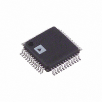
AD7641BSTZ Analog Devices Inc, AD7641BSTZ Datasheet - Page 8

AD7641BSTZ
Manufacturer Part Number
AD7641BSTZ
Description
IC ADC 18BIT 2MSPS SAR 48-LQFP
Manufacturer
Analog Devices Inc
Datasheet
1.AD7641BSTZ.pdf
(28 pages)
Specifications of AD7641BSTZ
Data Interface
Serial, Parallel
Number Of Bits
18
Sampling Rate (per Second)
2M
Number Of Converters
1
Power Dissipation (max)
92mW
Voltage Supply Source
Analog and Digital
Operating Temperature
-40°C ~ 85°C
Mounting Type
Surface Mount
Package / Case
48-LQFP
Resolution (bits)
18bit
Sampling Rate
2MSPS
Input Channel Type
Differential
Supply Current
23mA
Digital Ic Case Style
QFP
No. Of Pins
48
Lead Free Status / RoHS Status
Lead free / RoHS Compliant
For Use With
EVAL-AD7641CBZ - BOARD EVALUATION FOR AD7641
Lead Free Status / RoHS Status
Lead free / RoHS Compliant, Lead free / RoHS Compliant
Available stocks
Company
Part Number
Manufacturer
Quantity
Price
Company:
Part Number:
AD7641BSTZ
Manufacturer:
ADI
Quantity:
266
Company:
Part Number:
AD7641BSTZ
Manufacturer:
Analog Devices Inc
Quantity:
10 000
Company:
Part Number:
AD7641BSTZRL
Manufacturer:
Analog Devices Inc
Quantity:
10 000
AD7641
PIN CONFIGURATION AND FUNCTION DESCRIPTIONS
Table 6. Pin Function Descriptions
Pin
No.
1, 36,
41, 42
2, 44
3, 4
5
6
7
8
9
10
11, 12
Mnemonic
AGND
AVDD
MODE[0:1]
D0/OB/2C
WARP
NORMAL
D1/A0
D2/A1
D3
D[4:5]
or DIVSCLK[0:1]
Type
P
P
DI
DI/O
DI
DI
DI/O
DI/O
D0
DI/O
1
Description
Analog Power Ground Pin.
Input Analog Power Pins. Nominally 2.5 V.
Data Output Interface Mode Selection.
Interface MODE#
0
1
2
3
When MODE[1:0] = 0 (18-bit interface mode), this pin is Bit 0 of the parallel port data output bus
and the data coding is straight binary. In all other modes, this pin allows the choice of straight
binary/twos complement. When OB/ 2C is high, the digital output is straight binary; when low,
the MSB is inverted resulting in a twos complement output from its internal shift register.
Conversion Mode Selection. When WARP = high and NORMAL = high, this selects wideband warp
mode with slightly improved linearity and THD. When WARP = high and NORMAL = low, this selects
warp mode. In either mode, these are the fastest modes; maximum throughput is achievable, and
a minimum conversion rate must be applied to guarantee full specified accuracy.
Conversion Mode Selection. When NORMAL = low and WARP = low, this input selects normal mode
where full accuracy is maintained independent of the minimum conversion rate.
When MODE[1:0] = 0, this pin is Bit 1 of the parallel port data output bus. In all other modes, this
input pin controls the form in which data is output as shown in Table 7.
When MODE[1:0] = 0, this pin is Bit 2 of the parallel port data output bus.
When MODE[1:0] = 1 or 2, this input pin controls the form in which data is output as shown in Table 7.
When MODE[1:0] = 0, 1, or 2, this output is used as Bit 3 of the parallel port data output bus.
This pin is always an output, regardless of the interface mode.
When MODE[1:0] = 0, 1, or 2, these pins are Bit 4 and Bit 5 of the parallel port data output bus.
When MODE[1:0] = 3 (serial mode), serial clock division selection. When using serial master read
after convert mode (EXT/INT = low, RDC/SDIN = low), these inputs can be used to slow down the
internally generated serial clock that clocks the data output. In other serial modes, these pins are
high impedance outputs.
NC = NO CONNECT
D4/DIVSCLK[0]
D5/DIVSCLK[1]
D0/OB/2C
NORMAL
MODE0
MODE1
AGND
WARP
D1/A0
D2/A1
AVDD
D3
10
11
12
1
2
3
4
5
6
7
8
9
Figure 4. Pin Configuration
13 14 15 16 17 18 19 20 21 22 23 24
48 47 46 45 44
PIN 1
IDENTIFIER
Rev. 0 | Page 8 of 28
(Not to Scale)
TOP VIEW
AD7641
MODE1
0
0
1
1
43 42 41 40
39 38 37
MODE0
1
0
1
0
36
35
34
33
32
31
30
29
28
27
26
25
AGND
CNVST
PD
RESET
CS
RD
DGND
BUSY
D17
D16
D15
D14
Description
18-bit interface
16-bit interface
8-bit (byte) interface
Serial interface


