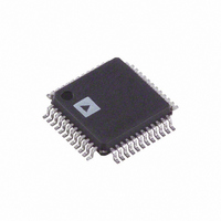
AD7641BSTZ Analog Devices Inc, AD7641BSTZ Datasheet - Page 22

AD7641BSTZ
Manufacturer Part Number
AD7641BSTZ
Description
IC ADC 18BIT 2MSPS SAR 48-LQFP
Manufacturer
Analog Devices Inc
Datasheet
1.AD7641BSTZ.pdf
(28 pages)
Specifications of AD7641BSTZ
Data Interface
Serial, Parallel
Number Of Bits
18
Sampling Rate (per Second)
2M
Number Of Converters
1
Power Dissipation (max)
92mW
Voltage Supply Source
Analog and Digital
Operating Temperature
-40°C ~ 85°C
Mounting Type
Surface Mount
Package / Case
48-LQFP
Resolution (bits)
18bit
Sampling Rate
2MSPS
Input Channel Type
Differential
Supply Current
23mA
Digital Ic Case Style
QFP
No. Of Pins
48
Lead Free Status / RoHS Status
Lead free / RoHS Compliant
For Use With
EVAL-AD7641CBZ - BOARD EVALUATION FOR AD7641
Lead Free Status / RoHS Status
Lead free / RoHS Compliant, Lead free / RoHS Compliant
Available stocks
Company
Part Number
Manufacturer
Quantity
Price
Company:
Part Number:
AD7641BSTZ
Manufacturer:
ADI
Quantity:
266
Company:
Part Number:
AD7641BSTZ
Manufacturer:
Analog Devices Inc
Quantity:
10 000
Company:
Part Number:
AD7641BSTZRL
Manufacturer:
Analog Devices Inc
Quantity:
10 000
AD7641
16-Bit and 8-Bit Interface (Master or Slave)
In the 16-bit (MODE[1:0] = 1) and 8-bit (MODE[1:0] = 2)
interfaces, the A0/A1 pins allow a glueless interface to a 16- or
8-bit bus, as shown in
address line(s), the data can be read in two words for a 16-bit
interface, or three bytes for an 8-bit interface. This interface can
be used in both master and slave parallel reading modes. Refer
to
CNVST,
CS = 0
D[17:10]
Figure 33. Slave Parallel Data Timing for Reading (Read During Convert)
BUSY
DATA
CS, RD
D[17:2]
Table 7 for the full details of the interface.
BUS
RD
A1
A0
HI-Z
HI-Z
Figure 34. 8-Bit and 16-Bit Parallel Interface
t
t
12
3
t
CONVERSION
12
BYTE
HIGH
Figure 34. By connecting A0/A1 to an
PREVIOUS
t
1
WORD
HIGH
t
13
t
12
BYTE
MID
t
4
t
WORD
BYTE
12
LOW
LOW
HI-Z
HI-Z
t
13
Rev. 0 | Page 22 of 28
SERIAL INTERFACE
The AD7641 is configured to use the serial interface when
MODE[1:0] = 3. The AD7641 outputs 18 bits of data, MSB first,
on the SDOUT pin. This data is synchronized with the 18 clock
pulses provided on the SCLK pin. The output data is valid on
both the rising and falling edge of the data clock.
MASTER SERIAL INTERFACE
Internal Clock
The AD7641 is configured to generate and provide the serial
data clock SCLK when the EXT/ INT pin is held low. The
AD7641 also generates a SYNC signal to indicate to the host
when the serial data is valid. The serial clock SCLK and the
SYNC signal can be inverted. Depending on the read during
convert input, RDC/SDIN, the data can be read after each
conversion or during the following conversion.
Figure 36 show detailed timing diagrams of these two modes.
Usually, because the AD7641 is used with a fast throughput, the
master read during conversion mode is the most recommended
serial mode. In this mode, the serial clock and data toggle at
appropriate instants, minimizing potential feedthrough between
digital activity and critical conversion decisions. In this mode,
the SCLK period changes because the LSBs require more time
to settle and the SCLK is derived from the SAR conversion cycle.
In read after conversion mode, it should be noted that unlike
other modes, the BUSY signal returns low after the 18 data bits
are pulsed out and not at the end of the conversion phase,
resulting in a longer BUSY width. As a result, the maximum
throughput cannot be achieved in this mode.
In addition, in read after convert mode, the SCLK frequency
can be slowed down to accommodate different hosts using the
DIVSCLK[1:0] inputs. Refer to
details when using these inputs.
Table 4 for the SCLK timing
Figure 35 and


