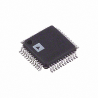
AD7641BSTZ Analog Devices Inc, AD7641BSTZ Datasheet - Page 21

AD7641BSTZ
Manufacturer Part Number
AD7641BSTZ
Description
IC ADC 18BIT 2MSPS SAR 48-LQFP
Manufacturer
Analog Devices Inc
Datasheet
1.AD7641BSTZ.pdf
(28 pages)
Specifications of AD7641BSTZ
Data Interface
Serial, Parallel
Number Of Bits
18
Sampling Rate (per Second)
2M
Number Of Converters
1
Power Dissipation (max)
92mW
Voltage Supply Source
Analog and Digital
Operating Temperature
-40°C ~ 85°C
Mounting Type
Surface Mount
Package / Case
48-LQFP
Resolution (bits)
18bit
Sampling Rate
2MSPS
Input Channel Type
Differential
Supply Current
23mA
Digital Ic Case Style
QFP
No. Of Pins
48
Lead Free Status / RoHS Status
Lead free / RoHS Compliant
For Use With
EVAL-AD7641CBZ - BOARD EVALUATION FOR AD7641
Lead Free Status / RoHS Status
Lead free / RoHS Compliant, Lead free / RoHS Compliant
Available stocks
Company
Part Number
Manufacturer
Quantity
Price
Company:
Part Number:
AD7641BSTZ
Manufacturer:
ADI
Quantity:
266
Company:
Part Number:
AD7641BSTZ
Manufacturer:
Analog Devices Inc
Quantity:
10 000
Company:
Part Number:
AD7641BSTZRL
Manufacturer:
Analog Devices Inc
Quantity:
10 000
INTERFACES
DIGITAL INTERFACE
The AD7641 has a versatile digital interface that can be set up
as either a serial or a parallel interface with the host system. The
serial interface is multiplexed on the parallel data bus. The AD7641
digital interface also accommodates 2.5 V, 3.3 V, or 5 V logic
with either OVDD at 2.5 V or 3.3 V. OVDD defines the logic
high output voltage. In most applications, the OVDD supply pin
of the AD7641 is connected to the host system interface 2.5 V
or 3.3 V digital supply. By using the D0/OB/
twos complement or straight binary coding can be used.
The two signals CS and RD control the interface. When at least
one of these signals is high, the interface outputs are in high
impedance. Usually, CS allows the selection of each AD7641 in
multicircuit applications and is held low in a single AD7641
design. RD is generally used to enable the conversion result on
the data bus.
RESET
The RESET input is used to reset the AD7641 and generate a
fast initialization. A rising edge on RESET aborts the current
conversion (if any) and tristates the data bus. The falling edge of
RESET clears the data bus and engages the initialization process
indicated by pulsing BUSY high. Conversions can take place
after the falling edge of BUSY. Refer to Figure 30 for the RESET
timing details.
CNVST
RESET
DATA
BUSY
t
9
t
38
Figure 30. RESET Timing
t
39
2C input pin, either
t
8
Rev. 0 | Page 21 of 28
PARALLEL INTERFACE
The AD7641 is configured to use the parallel interface for an
18-bit, 16-bit, or 8-bit bus width according to Table 7.
Master Parallel Interface
Data can be continuously read by tying CS
requiring minimal microprocessor connections. However, in
this mode, the data bus is always driven and cannot be used in
shared bus applications, unless the device is held in RESET.
Figure 31 details the timing for this mode.
CS = RD = 0
Slave Parallel Interface
In slave parallel reading mode, the data can be read either after
each conversion, which is during the next acquisition phase, or
during the following conversion, as shown in Figure 32 and
Figure 33, respectively. When the data is read during the
conversion, it is recommended that it is read-only during the
first half of the conversion phase. This avoids any potential
feedthrough between voltage transients on the digital interface
and the most critical analog conversion circuitry.
CNVST
BUSY
DATA
BUSY
DATA
BUS
BUS
Figure 31. Master Parallel Data Timing for Reading (Continuous Read)
Figure 32. Slave Parallel Data Timing for Reading (Read After Convert)
RD
CS
t
3
t
12
PREVIOUS CONVERSION DATA
t
1
CONVERSION
CURRENT
t
13
t
10
t
4
and
t
RD
11
low, thus
AD7641
NEW DATA


