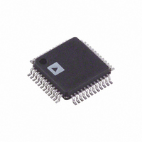
AD7641BSTZ Analog Devices Inc, AD7641BSTZ Datasheet - Page 11

AD7641BSTZ
Manufacturer Part Number
AD7641BSTZ
Description
IC ADC 18BIT 2MSPS SAR 48-LQFP
Manufacturer
Analog Devices Inc
Datasheet
1.AD7641BSTZ.pdf
(28 pages)
Specifications of AD7641BSTZ
Data Interface
Serial, Parallel
Number Of Bits
18
Sampling Rate (per Second)
2M
Number Of Converters
1
Power Dissipation (max)
92mW
Voltage Supply Source
Analog and Digital
Operating Temperature
-40°C ~ 85°C
Mounting Type
Surface Mount
Package / Case
48-LQFP
Resolution (bits)
18bit
Sampling Rate
2MSPS
Input Channel Type
Differential
Supply Current
23mA
Digital Ic Case Style
QFP
No. Of Pins
48
Lead Free Status / RoHS Status
Lead free / RoHS Compliant
For Use With
EVAL-AD7641CBZ - BOARD EVALUATION FOR AD7641
Lead Free Status / RoHS Status
Lead free / RoHS Compliant, Lead free / RoHS Compliant
Available stocks
Company
Part Number
Manufacturer
Quantity
Price
Company:
Part Number:
AD7641BSTZ
Manufacturer:
ADI
Quantity:
266
Company:
Part Number:
AD7641BSTZ
Manufacturer:
Analog Devices Inc
Quantity:
10 000
Company:
Part Number:
AD7641BSTZRL
Manufacturer:
Analog Devices Inc
Quantity:
10 000
TERMINOLOGY
Integral Nonlinearity Error (INL)
Linearity error refers to the deviation of each individual code
from a line drawn from negative full scale through positive full
scale. The point used as negative full scale occurs ½ LSB before
the first code transition. Positive full scale is defined as a level
1½ LSB beyond the last code transition. The deviation is
measured from the middle of each code to the true straight line.
Differential Nonlinearity Error (DNL)
In an ideal ADC, code transitions are 1 LSB apart. Differential
nonlinearity is the maximum deviation from this ideal value. It
is often specified in terms of resolution for which no missing
codes are guaranteed.
Gain Error
The first transition (from 000…00 to 000…01) should occur for
an analog voltage ½ LSB above the nominal negative full scale
(−2.0479922 V for the ±2.048 V range). The last transition
(from 111…10 to 111…11) should occur for an analog voltage
1½ LSB below the nominal full scale (+2.0479766 V for the
±2.048 V range). The gain error is the deviation of the
difference between the actual level of the last transition and the
actual level of the first transition from the difference between
the ideal levels.
Zero Error
The zero error is the difference between the ideal midscale
input voltage (0 V) and the actual voltage producing the
midscale output code.
Dynamic Range
It is the ratio of the rms value of the full scale to the rms noise
measured with the inputs shorted together. The value for
dynamic range is expressed in decibels.
Signal-to-Noise Ratio (SNR)
SNR is the ratio of the rms value of the actual input signal to the
rms sum of all other spectral components below the Nyquist
frequency, excluding harmonics and dc. The value for SNR is
expressed in decibels.
Rev. 0 | Page 11 of 28
Total Harmonic Distortion (THD)
THD is the ratio of the rms sum of the first five harmonic
components to the rms value of a full-scale input signal and is
expressed in decibels.
Signal to (Noise + Distortion) Ratio (SINAD)
SINAD is the ratio of the rms value of the actual input signal to
the rms sum of all other spectral components below the Nyquist
frequency, including harmonics but excluding dc. The value for
SINAD is expressed in decibels.
Spurious-Free Dynamic Range (SFDR)
The difference, in decibels (dB), between the rms amplitude of
the input signal and the peak spurious signal.
Effective Number of Bits (ENOB)
ENOB is a measurement of the resolution with a sine wave
input. It is related to SINAD and is expressed in bits by
Aperture Delay
Aperture delay is a measure of the acquisition performance and
is measured from the falling edge of the CNVST input to when
the input signal is held for a conversion.
Transient Response
The time required for the AD7641 to achieve its rated accuracy
after a full-scale step function is applied to its input.
Reference Voltage Temperature Coefficient
It is derived from the typical shift of output voltage at 25°C on a
sample of parts maximum and minimum reference output
voltage (V
expressed in ppm/°C using
where:
V
V
V
T
T
MAX
MIN
REF
REF
REF
(Max) = Maximum V
(Min) = Minimum V
(25°C) = V
ENOB = [(SINAD
= –40°C
TCV
= +85°C
REF
REF
) measured at T
(
ppm/
REF
at 25°C
°
C
)
dB
=
− 1.76)/6.02]
V
REF
REF
V
REF
REF
MIN
at T
at T
(
25
, T(25°C), and T
(
Max
MIN
°
MIN
C
, T(25°C), or T
)
, T(25°C), or T
×
)
−
(
T
V
MAX
REF
(
−
Min
T
MAX
MIN
)
MAX
. It is
MAX
)
AD7641
×
10
6


