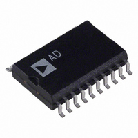
AD73311LAR Analog Devices Inc, AD73311LAR Datasheet - Page 13

AD73311LAR
Manufacturer Part Number
AD73311LAR
Description
IC ANALOG FRONT END 20-SOIC
Manufacturer
Analog Devices Inc
Datasheet
1.AD73311LAR.pdf
(36 pages)
Specifications of AD73311LAR
Rohs Status
RoHS non-compliant
Number Of Bits
16
Number Of Channels
2
Power (watts)
50mW
Voltage - Supply, Analog
3V
Voltage - Supply, Digital
3V
Package / Case
20-SOIC (7.5mm Width)
Single Supply Voltage (min)
2.7V
Single Supply Voltage (max)
3.3V
Package Type
SOIC W
Lead Free Status / RoHS Status
Not Compliant
Available stocks
Company
Part Number
Manufacturer
Quantity
Price
Part Number:
AD73311LAR
Manufacturer:
ADI/亚德诺
Quantity:
20 000
Company:
Part Number:
AD73311LARS
Manufacturer:
AD
Quantity:
12
Part Number:
AD73311LARS
Manufacturer:
ADI/亚德诺
Quantity:
20 000
Company:
Part Number:
AD73311LARS/AD73311
Manufacturer:
LITEON
Quantity:
10 000
Company:
Part Number:
AD73311LARSREEL
Manufacturer:
STM
Quantity:
6 706
Company:
Part Number:
AD73311LARSZ
Manufacturer:
MIC
Quantity:
6 222
Part Number:
AD73311LARSZ
Manufacturer:
ADI/亚德诺
Quantity:
20 000
Part Number:
AD73311LARSZ-REEL
Manufacturer:
ADI/亚德诺
Quantity:
20 000
Part Number:
AD73311LARU
Manufacturer:
ADI/亚德诺
Quantity:
20 000
Control
Bit 15
Bit 14
Bits 13–11
Bits 10–8
Bits 7–0
DA4
0
0
0
—
1
1
OPERATION
Resetting the AD73311L
The pin RESET resets all the control registers. All registers are
reset to zero indicating that the default SCLK rate (DMCLK/8)
and sample rate (DMCLK/2048) are at a minimum to ensure
that slow speed DSP engines can communicate effectively. As
well as resetting the control registers using the RESET pin, the
device can be reset using the RESET bit (CRA:7) in Control
Register A. Both hardware and software resets require 4 DMCLK
cycles. On reset, DATA/PGM (CRA:0) is set to 0 (default condi-
tion) thus enabling Program Mode. The reset conditions ensure
Address (Binary)
000
001
010
011
100
101
110 to 111
DMCLK = 16.384 MHz.
C/D
15
DA3
0
0
0
—
1
1
R/W
14
Table VIII. DAC Timing Control
Frame
Control/Data
Read/Write
Device Address
Register Address
Register Data
DA2
0
0
0
—
1
1
13
Device Address
DA1
0
0
1
—
1
1
12
Name
CRA
CRB
CRC
CRD
CRE
CRF
11
DA0
0
1
0
—
0
1
Description
When set high, it signifies a control word in Program or Mixed Program/Data Modes. When
set low, it signifies a data word in Mixed Program/Data Mode or an invalid control word in
Program Mode.
When set low, it tells the device that the data field is to be written to the register selected by
the register field setting provided the address field is zero. When set high, it tells the device
that the selected register is to be written to the data field in the input serial register and that
the new control word is to be output from the device via the serial output.
This 3-bit field holds the address information. Only when this field is zero is a device selected.
If the address is not zero, it is decremented and the control word is passed out of the device
via the serial output.
the address field is zero.
This 3-bit field is used to select one of the five control registers on the AD73311L.
This 8-bit field holds the data that is to be written to or read from the selected register provided
10
Register Address
Time Advance
0 ns
488.2 ns
976.5 ns
—
14.64 µs
15.13 µs
Description
Control Register A
Control Register B
Control Register C
Control Register D
Control Register E
Control Register F
Reserved
Table X. Control Word Description
Table IX. Control Register Map
9
8
that the device must be programmed to the correct settings after
power-up or reset. Following a reset, the SDOFS will be asserted
2048 DMCLK cycles after RESET going high. The data that
is output following RESET and during Program Mode is ran-
dom and contains no valid information until either Data or
Mixed Mode is set.
Power Management
The individual functional blocks of the AD73311L can be
enabled separately by programming the power control register
CRC. It allows certain sections to be powered down if not
required, which adds to the device’s flexibility in that the user
need not incur the penalty of having to provide power for a
certain section if it is not necessary to their design. The power
control register provides individual control settings for the major
functional blocks and also a global override that allows all sec-
tions to be powered up by setting the bit. Using this method the
user could, for example, individually enable a certain section,
such as the reference (CRC:5), and disable all others. The glo-
bal power-up (CRC:0) can be used to enable all sections but if
power-down is required using the global control, the reference
will still be enabled, in this case, because its individual bit is set.
Refer to Table XIII for details of the settings of CRC.
7
6
Type
R/W
R/W
R/W
R/W
R/W
R/W
5
Register Data
4
Width
8
8
8
8
8
8
3
2
Reset Setting (Hex)
0x00
0x00
0x00
0x00
0x00
0x00
AD73311L
1
0


