ISL12032IVZ Intersil, ISL12032IVZ Datasheet - Page 17
ISL12032IVZ
Manufacturer Part Number
ISL12032IVZ
Description
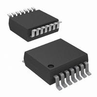
IC RTC LP BATT BACK SRAM 14TSSOP
Manufacturer
Intersil
Type
Clock/Calendar/NVSRAMr
Datasheet
1.ISL12032IVZ-T.pdf
(26 pages)
Specifications of ISL12032IVZ
Memory Size
1K (128 x 8)
Time Format
HH:MM:SS:hh (12/24 hr)
Date Format
YY-MM-DD-dd
Interface
I²C, 2-Wire Serial
Voltage - Supply
2.7 V ~ 5.5 V
Operating Temperature
-40°C ~ 85°C
Mounting Type
Surface Mount
Package / Case
14-TSSOP
Lead Free Status / RoHS Status
Lead free / RoHS Compliant
Available stocks
Company
Part Number
Manufacturer
Quantity
Price
Company:

Part Number:
ISL12032IVZ-T
Manufacturer:
Intersil
Quantity:
11 856


I
Where the R
VBAT. Table 14 gives the typical resistor values for V
and VBAT = 3.0V. Note that the resistor value changes with
V
temperature.
Power Supply Control Register (PWRVDD)
CLEAR TIME STAMP BIT (CLRTS)
This bit clears both the Time Stamp V
and Time Stamp Battery to V
default setting is “0” which allows normal operation. Setting
CLRTS = 1 performs the clear timestamp register function at
the conclusion of a successful write operation.
I
This bit allows I
powered) when set to “1”. When reset to “0”, the I
operation is disabled in battery mode, which results in the
lowest I
Note that when the I
the SCL and SDA pull-ups must go to the VBAT source for
proper communications. This will result in additional VBAT
current drain (on top of the increased device VBAT current)
during serial communications.
V
These bits set the 6 trip levels for the V
switchover. The LVDD bit in the SRDC is set to “1” when
V
MAX
2
TABLE 15. POWER SUPPLY CONTROL REGISTER (PWRVDD)
ADDR
DD
DD
DD
C IN BATTERY MODE (I2CBAT)
11h
V
TRKRO1
DD
input voltage and VBAT voltage, as well as with
BROWNOUT TRIP VOLTAGE (VDDTRIP <2:0>)
drops below this preset level. See Table 16.
=
0
0
0
0
0
1
1
Trip2
DD
V
-------------------------------- -
TABLE 14. RESISTOR SELECTION REGISTER
CLRTS
DD
R
current.
7
OUT
–
OUT
V
BAT
2
TABLE 16. VDD TRIP LEVELS
C operation in battery backup mode (VBAT
is the selected resistor between V
X
TRKRO0
6
V
DD
2
C operation is desired in VBAT mode,
0
1
0
1
I2CBAT
0
0
1
Trip1
5
17
DD
LVENB
(TSB2V) sections. The
V
4
DD
1300
2200
3600
7800
Rtrk
0
1
0
DD
Trip0
DD
to Battery (TSV2B)
3
X
alarm and VBAT
Trip2
VDD
2
VOLTAGE
2
UNITS
2.295
2.550
2.805
C
TRIP
Trip1
VDD
DD
(V)
DD
Ω
Ω
Ω
Ω
1
(EQ. 1)
and
= 5V
Trip0
VDD
0
ISL12032
Battery Voltage Warning Register (PWRVBAT)
This register controls the trip points for the two VBAT
warnings, with levels set to approximately 85% and 75% of
the nominal battery level.
VBAT HYSTERESIS (BHYS)
This bit enables/disables the hysteresis voltage for the
V
and switching to VBAT occurs at approximately 50mV below
the V
VBAT to V
the V
When set to “0”, there is no hysteresis and switchover will
occur at exactly the VDD trip point. Note that for slow moving
V
extra switching cycles without hysteresis.
BATTERY LEVEL MONITOR TRIP BITS (VB85TP <2:0>)
Three bits selects the first alarm (85% of Nominal VBAT) level
for the battery voltage monitor. There are total of 7 levels that
could be selected for the first warning. Any of the levels could
be selected as the first warning with no reference as to nominal
VBAT voltage level. See Table 18 for typical values.
ADDR
TABLE 17. BATTERY VOLTAGE WARNING REGISTER
DD
DD
12h
V
DD
/VBAT switchover. When set to “1”, hysteresis is enabled
DD
DD
power-down and power-up signals there can be some
0
1
1
Trip2
Trip point (set by VDDTrip<2:0>). Switching from
trip point.
7
X BHYS VB85T
DD
(PWRVBAT)
power will occur at approximately 50mV above
6
TABLE 16. VDD TRIP LEVELS
V
DD
p2
5
1
0
0
Trip1
VB85T
p1
4
V
VB85T
DD
p0
3
Trip0
1
0
1
VB75T
p2
2
VOLTAGE
VB75T
3.060
4.250
4.675
TRIP
p1
April 16, 2009
1
(V)
FN6618.2
VB75T
p0
0
Related parts for ISL12032IVZ
Image
Part Number
Description
Manufacturer
Datasheet
Request
R

Part Number:
Description:
Intersil Corporation [CMOS Serial Controller Interface]
Manufacturer:
Intersil Corporation
Datasheet:
Part Number:
Description:
Manufacturer:
Intersil Corporation
Datasheet:
Part Number:
Description:
357-036-542-201 CARDEDGE 36POS DL .156 BLK LOPRO
Manufacturer:
Intersil Corporation
Datasheet:
Part Number:
Description:
1024-Word x 4-Bit LSI Static RAM
Manufacturer:
Intersil Corporation
Datasheet:
Part Number:
Description:
General Purpose NPN Transistor Arrays FN341.4
Manufacturer:
Intersil Corporation
Datasheet:
Part Number:
Description:
CMOS 16-Bit Microprocessor
Manufacturer:
Intersil Corporation
Datasheet:
Part Number:
Description:
Manufacturer:
Intersil Corporation
Datasheet:
Part Number:
Description:
Manufacturer:
Intersil Corporation
Datasheet:
Part Number:
Description:
Manufacturer:
Intersil Corporation
Datasheet:
Part Number:
Description:
Manufacturer:
Intersil Corporation
Datasheet:
Part Number:
Description:
CMOS 6-Bit Latch and Decoder Memory Interfaces
Manufacturer:
Intersil Corporation
Datasheet:
Part Number:
Description:
CA3046General Purpose NPN Transistor Arrays
Manufacturer:
Intersil Corporation
Datasheet:
Part Number:
Description:
Manufacturer:
Intersil Corporation
Datasheet:
Part Number:
Description:
TR909 DLC/FLC SLIC with Low Power Standby
Manufacturer:
Intersil Corporation
Datasheet:
Part Number:
Description:
Manufacturer:
Intersil Corporation
Datasheet: