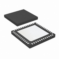
LMK03002CISQ/NOPB National Semiconductor, LMK03002CISQ/NOPB Datasheet - Page 6

LMK03002CISQ/NOPB
Manufacturer Part Number
LMK03002CISQ/NOPB
Description
IC CLOCK CONDITIONER PLL 48-LLP
Manufacturer
National Semiconductor
Type
Clock Conditionerr
Datasheet
1.LMK03002ISQNOPB.pdf
(26 pages)
Specifications of LMK03002CISQ/NOPB
Pll
Yes
Input
Clock
Output
LVPECL
Number Of Circuits
1
Ratio - Input:output
1:4
Differential - Input:output
Yes/Yes
Frequency - Max
1.724GHz
Divider/multiplier
Yes/No
Voltage - Supply
3.15 V ~ 3.45 V
Operating Temperature
-40°C ~ 85°C
Mounting Type
Surface Mount
Package / Case
48-LLP
Frequency-max
1.724GHz
For Use With
LMK03002CEVAL - PRECISION CLOCK CONDITIONER WITH
Lead Free Status / RoHS Status
Lead free / RoHS Compliant
Other names
LMK03002CISQTR
www.national.com
Jitter
t
V
V
V
V
V
I
I
V
V
V
V
I
I
t
t
t
t
t
t
t
SKEW
IH
IL
IH
IL
CS
CH
CWH
CWL
ES
CES
EWH
OH
OL
OD
IH
IL
OH
OL
IH
IL
Note 4: The Electrical Characteristics table lists guaranteed specifications under the listed Recommended Operating Conditions except as otherwise modified
or specified by the Electrical Characteristics Conditions and/or Notes. Typical specifications are estimations only and are not guaranteed.
Note 5: See 3.5 for more current consumption / power dissipation calculation information.
Note 6: A specification in modeling PLL in-band phase noise is the 1/f flicker noise, L
dB/decade slope. PN10kHz is normalized to a 10 kHz offset and a 1 GHz carrier frequency. PN10kHz = L
(f) is the single side band phase noise of only the flicker noise's contribution to total noise, L(f). To measure L
slope close to the carrier. A high compare frequency and a clean crystal are important to isolating this noise source from the total phase noise, L(f). L
can be masked by the reference oscillator performance if a low power or noisy source is used. The total PLL inband phase noise performance is the sum of
L
Note 7: A specification in modeling PLL in-band phase noise is the Normalized Phase Noise Contribution, L
L
detector frequency of the synthesizer. L
smaller then the loop bandwidth of the PLL, and yet large enough to avoid a substantial noise contribution from the reference and flicker noise. L
masked by the reference oscillator performance if a low power or noisy source is used.
Note 8: Allowable Temperature Drift for Continuous Lock is how far the temperature can drift in either direction and stay in lock from the ambient temperature
and programmed state at which the device was when register R15 was programmed. The action of programming the R15 register, even to the same value,
activates a frequency calibration routine. This implies that the device will work over the entire frequency range, but if the temperature drifts more than the maximum
allowable drift for continuous lock, then it will be necessary to reprogram the R15 register to ensure that the device stays in lock. Regardless of what temperature
the device was initially programmed at, the ambient temperature can never drift outside the range of -40 °C
this specification to be valid, the programmed state of the device must not change after R15 is programmed.
Symbol
PLL_flicker
PLL_flat
ADD
(f) – 20log(N) – 10log(f
(f) and L
Additive RMS Jitter
CLKoutX to CLKoutY
Output High Voltage
Output Low Voltage
Differential Output Voltage
High-Level Input Voltage
Low-Level Input Voltage
High-Level Input Current
Low-Level Input Current
High-Level Output Voltage
Low-Level Output Voltage
High-Level Input Voltage
Low-Level Input Voltage
High-Level Input Current
Low-Level Input Current
Data to Clock Set Up Time
Data to Clock Hold Time
Clock Pulse Width High
Clock Pulse Width Low
Clock to Enable Set Up Time
Enable to Clock Set Up Time
Enable Pulse Width High
PLL_flat
(f).
COMP
). L
Parameter
PLL_flat
Clock Distribution Section
PLL_flat
(Note
(Note
(f) is the single side band phase noise measured at an offset frequency, f, in a 1 Hz Bandwidth and f
(f) contributes to the total noise, L(f). To measure L
10)
11)
Digital MICROWIRE Interfaces
Digital LVTTL Interfaces
MICROWIRE Timing
R
Distribution Path =
800 MHz
Bandwidth =
12 kHz to 20 MHz
Equal loading and identical clock
configuration
Termination = 50 Ω to Vcc - 2 V
Termination = 50 Ω to Vcc - 2 V
CLKoutX output frequency = 200 MHz
V
V
I
I
V
V
See Data Input Timing
See Data Input Timing
See Data Input Timing
See Data Input Timing
See Data Input Timing
See Data Input Timing
See Data Input Timing
OH
OL
IH
IL
IH
IL
L
= 100 Ω
= -500 µA
= 0
= 0
= Vcc
= +500 µA
= Vcc
(Note
6
10) - LVPECL Clock Outputs
PLL_flicker
Conditions
(Note
(f), which is dominant close to the carrier. Flicker noise has a 10
(Note
CLKoutX_MUX
= Bypass
CLKoutX_MUX
= Divided
CLKoutX_DIV =
4
PLL_flat
12)
13)
(f) the offset frequency, f, must be chosen sufficiently
PLL_flicker
≤
PLL_flat
PLL_flicker
T
A
(10 kHz) - 20log(Fout / 1 GHz), where L
≤
(f), of the PLL and is defined as PN1Hz =
85 °C without violating specifications. For
(f) it is important to be on the 10 dB/decade
-40.0
Vcc -
Min
-5.0
-5.0
-5.0
660
-30
2.0
0.4
1.6
25
25
25
25
25
25
8
Vcc -
Vcc -
0.98
Typ
810
1.8
±3
20
75
COMP
Max
965
Vcc
Vcc
PLL_flat
0.8
5.0
5.0
0.4
0.4
5.0
5.0
30
is the phase
PLL_flicker
(f) can be
PLL_flicker
Units
mV
µA
µA
µA
µA
ps
ns
ns
ns
ns
ns
ns
ns
fs
V
V
V
V
V
V
V
V
(f)


