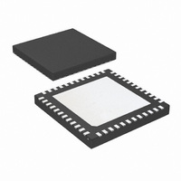
LMK03002CISQ/NOPB National Semiconductor, LMK03002CISQ/NOPB Datasheet

LMK03002CISQ/NOPB
Specifications of LMK03002CISQ/NOPB
Related parts for LMK03002CISQ/NOPB
LMK03002CISQ/NOPB Summary of contents
Page 1
... The clock conditioners come in a 48-pin LLP package and are footprint compatible with other clocking devices in the same family. System Diagram TRI-STATE ® registered trademark of National Semiconductor Corporation. © 2010 National Semiconductor Corporation LMK03002/LMK03002C Features ■ Integrated VCO with very low phase noise floor ■ ...
Page 2
Functional Block Diagram www.national.com 2 30020601 ...
Page 3
Connection Diagram Pin Descriptions Pin # 13, 16, 19, 22, 26, Vcc1, Vcc2, Vcc3, Vcc4, Vcc5, Vcc6, Vcc7, Vcc8, 30, 31, 33, 37, 40, 43, 46 Vcc9, Vcc10, Vcc11, Vcc12, Vcc13, Vcc14 ...
Page 4
... Absolute Maximum Ratings If Military/Aerospace specified devices are required, please contact the National Semiconductor Sales Office/ Distributors for availability and specifications. Parameter Power Supply Voltage Input Voltage Storage Temperature Range Lead Temperature (solder 4 s) Junction Temperature Recommended Operating Conditions Parameter Ambient Temperature Power Supply Voltage Note 1: " ...
Page 5
Symbol Parameter I CPout Charge Pump Sink Current SINK I TRI Charge Pump TRI-STATE CPout Magnitude of Charge Pump I %MIS CPout Sink vs. Source Current Mismatch Magnitude of Charge Pump I VTUNE Current vs. Charge Pump Voltage CPout Variation ...
Page 6
Symbol Parameter Clock Distribution Section Jitter Additive RMS Jitter (Note ADD t CLKoutX to CLKoutY (Note SKEW V Output High Voltage OH V Output Low Voltage OL V Differential Output Voltage OD V High-Level Input Voltage IH V Low-Level Input ...
Page 7
Note 9: VCO phase noise is measured assuming the VCO is the dominant noise source due loop bandwidth. Over frequency, the phase noise typically varies dB, with the worst case performance typically ...
Page 8
Charge Pump Current Specification Definitions I1 = Charge Pump Sink Current Charge Pump Sink Current Charge Pump Sink Current Charge Pump Source Current Charge ...
Page 9
Typical Performance Characteristics LVPECL Differential Output Voltage (V Delay Noise Floor (Adds to Output Noise Floor) ) LVPECL Output Noise Floor OD 30020608 30020611 9 30020610 www.national.com ...
Page 10
Functional Description The LMK03002/LMK03002C precision clock conditioners combine the functions of jitter cleaning/reconditioning, multi- plication, and distribution of a reference clock. The devices integrate a Voltage Controlled Oscillator (VCO), a high per- formance Integer-N Phase Locked Loop (PLL), a ...
Page 11
CLKout OUTPUT STATES Each clock output may be individually enabled with the CLKoutX_EN bits. Each individual output enable control bit is gated with the Global Output Enable input pin (GOE) and the Global Output Enable bit (EN_CLKout_Global). All clock ...
Page 12
General Programming Information The LMK03002/LMK03002C devices are programmed using several 32-bit registers which control the device's operation. The registers consist of a data field and an address field. The last 4 register bits, ADDR[3:0] form the address field. The ...
Page 13
CLKout0_EN CLKout1_EN CLKout2_EN CLKout3_EN RESET Register DIV4 Vboost 13 www.national.com ...
Page 14
POWERDOWN EN_CLKout_Global EN_Fout Register www.national.com 14 ...
Page 15
REGISTERS R0 Registers R4 through R7 control the four clock outputs. Reg- ister R3 controls CLKout0, Register R4 controls CLKout1, and so on. There is one additional bit in register R0 called RESET. Default Bit Name ...
Page 16
CLKoutX_DLY[3:0] -- Clock Output Delays These bits control the delay stages for each clock output. In order for these delays to be active, the respective CLKoutX_MUX (See 2.3.2) bit must be set to either "Delayed" or "Divided and Delayed" ...
Page 17
VCO_R4_LF[2:0] -- Value for Internal Loop Filter Resistor R4 These bits control the R4 resistor value in the internal loop filter. The recommended setting for VCO_R4_LF[2: for optimum phase noise and jitter. VCO_R4_LF[2:0] R4 Value (kΩ) Low ...
Page 18
POWERDOWN bit -- Device Power Down This bit can power down the device. Enabling this bit powers down the entire device and all blocks, regardless of the state of any of the other bits or pins. POWERDOWN bit 0 ...
Page 19
Application Information 3.1 SYSTEM LEVEL DIAGRAM Figure 3 shows an LMK03000 family device used in a typical application. In this setup the clock may be multiplied, recon- ditioned, and redistributed. Both the OSCin/OSCin* and CLK- outX/CLKoutX* pins can be ...
Page 20
LOOP FILTER The internal charge pump is directly connected to the inte- grated loop filter components. The first and second pole of the loop filter are externally attached as shown in the loop filter is designed, it must be ...
Page 21
CURRENT CONSUMPTION / POWER DISSIPATION CALCULATIONS Due to the myriad of possible configurations the following ta- ble serves to provide enough information to allow the user to Table 3.5 - Block Current Consumption Block Condition Entire device, All outputs ...
Page 22
THERMAL MANAGEMENT Power consumption of the LMK03002/LMK03002C devices can be high enough to require attention to thermal manage- ment. For reliability and performance reasons the die tem- perature should be limited to a maximum of 125 °C. That is, ...
Page 23
FIGURE 7. Differential LVPECL Operation, DC Coupling, Thevenin Equivalent 3.7.2 Termination for AC Coupled Differential Operation AC coupling allows for shifting the DC bias level (common mode voltage) when driving different receiver standards. Since AC coupling prevents the driver from ...
Page 24
OSCin INPUT In addition to LVDS and LVPECL inputs, OSCin can also be driven with a sine wave. The OSCin input can be driven sin- gle-ended or differentially with sine waves. The configurations for these are shown in Figure ...
Page 25
Physical Dimensions inches (millimeters) unless otherwise noted Ordering Information Order Number Package Marking LMK03002ISQ K03002 I LMK03002ISQX K03002 I LMK03002CISQ K03002CI LMK03002CISQX K03002CI Leadless Leadframe Package (Bottom View) 48 Pin LLP (SQA48A) Package Packing VCO Version 250 Unit Tape and ...
Page 26
... For more National Semiconductor product information and proven design tools, visit the following Web sites at: www.national.com Products Amplifiers www.national.com/amplifiers Audio www.national.com/audio Clock and Timing www.national.com/timing Data Converters www.national.com/adc Interface www.national.com/interface LVDS www.national.com/lvds Power Management www.national.com/power Switching Regulators www.national.com/switchers LDOs www.national.com/ldo LED Lighting www ...


