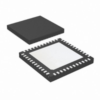
LMK03002CISQ/NOPB National Semiconductor, LMK03002CISQ/NOPB Datasheet - Page 21

LMK03002CISQ/NOPB
Manufacturer Part Number
LMK03002CISQ/NOPB
Description
IC CLOCK CONDITIONER PLL 48-LLP
Manufacturer
National Semiconductor
Type
Clock Conditionerr
Datasheet
1.LMK03002ISQNOPB.pdf
(26 pages)
Specifications of LMK03002CISQ/NOPB
Pll
Yes
Input
Clock
Output
LVPECL
Number Of Circuits
1
Ratio - Input:output
1:4
Differential - Input:output
Yes/Yes
Frequency - Max
1.724GHz
Divider/multiplier
Yes/No
Voltage - Supply
3.15 V ~ 3.45 V
Operating Temperature
-40°C ~ 85°C
Mounting Type
Surface Mount
Package / Case
48-LLP
Frequency-max
1.724GHz
For Use With
LMK03002CEVAL - PRECISION CLOCK CONDITIONER WITH
Lead Free Status / RoHS Status
Lead free / RoHS Compliant
Other names
LMK03002CISQTR
3.5 CURRENT CONSUMPTION / POWER DISSIPATION
CALCULATIONS
Due to the myriad of possible configurations the following ta-
ble serves to provide enough information to allow the user to
From Table 3.5 the current consumption can be calculated in
any configuration. For example, the current for the entire de-
vice with two LVPECL (CLKout0 and CLKout3) outputs in
bypass mode can be calculated by adding up the following
blocks: core current, clock buffers, and two LVPECL output
buffer currents. There will also be two LVPECL outputs draw-
ing emitter current, but some of the power from the current
draw is dissipated in the external 120 Ω resistors which
doesn't add to the power dissipation budget for the device. If
delays or divides are switched in, then the additional current
for these stages needs to be added as well.
For power dissipated by the device, the total current entering
the device is multiplied by the voltage at the device minus the
power dissipated in any emitter resistors connected to any of
the LVPECL outputs. If no emitter resistors are connected to
Table 3.5 - Block Current Consumption
Block
Entire device,
core current
Clock buffers
(internal)
Output buffers
Divide circuitry
per output
Delay circuitry
per output
Entire device
Condition
All outputs off; No LVPECL emitter resistors connected
The clock buffers are enabled anytime one of CLKout0
through CLKout3 are enabled
Fout buffer, EN_Fout = 1
LVPECL output, bypass mode (includes 120 Ω emitter
resistors)
LVPECL output, disabled mode (includes 120 Ω
emitter resistors)
LVPECL output, disabled mode. No emitter resistors
placed; open outputs
Divide enabled, divide = 2
Divide enabled, divide > 2
Delay enabled, delay < 8
Delay enabled, delay > 7
CLKout0 & CLKout3 enabled in bypass mode
21
calculate estimated current consumption of the device. Un-
less otherwise noted Vcc = 3.3 V, T
the LVPECL outputs, this power will be 0 watts. For example,
in the case of two LVPECL (CLKout0 & CLKout3) outputs op-
erating at 3.3 volts, we calculate 3.3 V × (86 + 9 + 40 + 40)
mA = 3.3 V × 175 mA = 577.5 mW. Because two LVPECL
outputs (CLKout0 and CLKout3) have the emitter resistors
hooked up and the power dissipated by these resistors is 60
mW for each clock, the total device power dissipation is 533.9
mW - 120 mW = 457.5 mW.
When the LVPECL output is active, ~1.9 V is the average
voltage on each output as calculated from the LVPECL V
& V
each emitter resistor is approximately (1.9 V)
mW. When the LVPECL output is disabled, the emitter resis-
tor voltage is ~1.07 V. Therefore the power dissipated in each
emitter resistor is approximately (1.07 V)
OL
Consumption at
typical specification. Therefore the power dissipated in
3.3 V (mA)
Current
86.0
14.5
17.4
175
5.3
8.5
5.8
9.9
40
9
0
Dissipated in
device (mW)
Power
283.8
457.5
29.7
47.8
38.3
17.5
28.0
19.1
32.7
72
0
A
= 25 °C.
2
/ 120 Ω = 9.5 mW.
LVPECL emitter
resistors (mW)
Dissipated in
2
/ 120 Ω = 30
Power
www.national.com
19.1
120
60
-
-
-
-
-
-
-
-
OH


