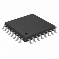
MAX3676EHJ Maxim Integrated Products, MAX3676EHJ Datasheet - Page 11

MAX3676EHJ
Manufacturer Part Number
MAX3676EHJ
Description
IC RECOV/RETIME 622MBPS 32-TQFP
Manufacturer
Maxim Integrated Products
Type
Clock and Data Recovery (CDR)r
Datasheet
1.MAX3676EHJ.pdf
(15 pages)
Specifications of MAX3676EHJ
Input
PECL
Output
PECL
Frequency - Max
622MHz
Voltage - Supply
3 V ~ 5.5 V
Operating Temperature
-40°C ~ 85°C
Mounting Type
Surface Mount
Package / Case
32-TQFP, 32-VQFP
Frequency-max
622MHz
Lead Free Status / RoHS Status
Contains lead / RoHS non-compliant
Available stocks
Company
Part Number
Manufacturer
Quantity
Price
Part Number:
MAX3676EHJ
Manufacturer:
MAXIM/美信
Quantity:
20 000
Company:
Part Number:
MAX3676EHJ+
Manufacturer:
MAXIM
Quantity:
67
Company:
Part Number:
MAX3676EHJ+
Manufacturer:
Maxim Integrated
Quantity:
10 000
Company:
Part Number:
MAX3676EHJ+T
Manufacturer:
Maxim Integrated
Quantity:
10 000
Part Number:
MAX3676EHJ+T
Manufacturer:
MAXIM/美信
Quantity:
20 000
Company:
Part Number:
MAX3676EHJ-T
Manufacturer:
Maxim Integrated
Quantity:
10 000
The limiting amplifier is biased independently from the
clock recovery circuitry. Grounding INSEL turns off the
limiting amplifier and selects the PECL DDI inputs.
Many of the MAX3676’s specifications relate to input-
signal amplitude. When working with fiber optic
receivers, the input is usually expressed in terms of
average optical power and extinction ratio. The rela-
tions given in Table 2 and Figure 6 are helpful for con-
verting optical power to input signal when designing
with the MAX3676.
In an optical receiver, the input voltage to the limiting
amplifier can be found by multiplying the relationship in
Table 2 by the photodiode responsivity and transim-
pedance amplifier gain.
Power and hysteresis are often expressed in decibels.
By definition, decibels are always 10log (power). At the
inputs to the MAX3676 limiting amplifier, the power is
V
by a factor of two, and the preamplifier is linear, then the
voltage at the input to the MAX3676 also increases by a
factor of two.
The optical power increase is:
At the MAX3676, the voltage increase is:
Table 2. Optical-Power Relations*
*Assuming a 50% average input-data duty cycle.
IN
PARAMETER
Average
Power
Extinction
Ratio
Optical Power
of a “1”
Optical Power
of a “0”
Signal
Amplitude
10
2
/R. If a receiver’s optical input power (x) increases
log
(
10log(2x/x) = 10log(2) = +3dB
2V
Converting Average Optical Power
V
IN
IN
2
)
/ R
2
Without the Limiting Amplifier
SYMBOL
Reduced Power Consumption
/ R
Data-Retiming IC with Limiting Amplifier
______________________________________________________________________________________
P
P
AVG
P1
P0
r
e
IN
=
10
log(
P
P
r = 1 / P0
P0 2P
P
e
1 2
IN
AVG
to Signal Amplitude
2
622Mbps, 3.3V Clock-Recovery and
=
=
2
Optical Hysteresis
=
P
)
P
P
= P0 + P1 / 2
=
AVG
1
AVG
(
−
20
RELATION
P
0 2
r
log(
e
/ r
r
=
e
( )
+
e
1
2
P
+
)
AVG
) ) = +6dB
1
(
r
r
e
e
−
+
1
1
)
In an optical receiver, the decibel change at the
MAX3676 always equals 2x the optical decibel change.
The MAX3676’s typical voltage hysteresis is 3.0dB. This
provides an optical hysteresis of 1.5dB.
Timing jitter, edge speeds, aberrations, optical disper-
sion, and attenuation all impact the performance of
high-speed clock recovery for SDH/SONET receivers
(Figure 7). These effects decrease the time available
for error-free data recovery by reducing the received
“eye opening” of nonreturn-to-zero (NRZ) transmitted
signals.
Figure 6. Optical Power Relations
Figure 7. Eye Diagram With and Without Timing Jitter
P
AVE
P1
P0
EFFECTS OF TIMING JITTER ON EYE DIAGRAM
EYE DIAGRAM WITH NO TIMING JITTER
Jitter in Optical Receivers
TIME
MIDPOINT
MIDPOINT
TIME
TIME
11


