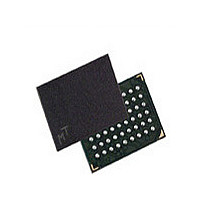
MT45W2MW16BGB-701 IT Micron Technology Inc, MT45W2MW16BGB-701 IT Datasheet - Page 20

MT45W2MW16BGB-701 IT
Manufacturer Part Number
MT45W2MW16BGB-701 IT
Description
Manufacturer
Micron Technology Inc
Datasheet
1.MT45W2MW16BGB-701_IT.pdf
(61 pages)
Specifications of MT45W2MW16BGB-701 IT
Operating Temperature (max)
85C
Operating Temperature (min)
-40C
Mounting
Surface Mount
Operating Temperature Classification
Industrial
Lead Free Status / RoHS Status
Compliant
Configuration Registers
Access Using CRE
Figure 13:
PDF: 09005aef82832fa2/Source: 09005aef82832f5f
32mb_burst_cr1_0_p24z_2.fm - Rev. E 9/08 EN
(except A19)
DQ[15:0]
LB#/UB#
A[20:0]
ADV#
A19
WE#
OE#
CLK
CRE
CE#
1
Asynchronous Mode Configuration Register WRITE Followed by READ ARRAY Operation
Note:
Note:
t VPH
Select control register
Two user-accessible configuration registers define the device operation. The bus config-
uration register (BCR) defines how the CellularRAM interacts with the system memory bus
and is nearly identical to its counterpart on burst mode Flash devices. The refresh configu-
ration register (RCR) is used to control how refresh is performed on the DRAM array.
These registers are automatically loaded with default settings during power-up and can
be updated any time the devices are operating in a standby state.
The configuration registers are loaded using either a synchronous or an asynchronous
WRITE operation when the configuration register enable (CRE) input is HIGH (see
Figure 13, and Figure 14 on page 21). When CRE is LOW, a READ or WRITE operation
will access the memory array. The register values are placed on address pins A[19:0]. In
an asynchronous WRITE, the values are latched into the configuration register on the
rising edge of ADV#, CE#, or WE#, whichever occurs first; LB# and UB# are “Don’t Care.”
The BCR is accessed when A[19] is HIGH; the RCR is accessed when A[19] is LOW. For
READs, address inputs other than A19 are “Don't Care,” and register bits 15:0 are output
on DQ[15:0].
A[19] = LOW to load RCR, HIGH to load BCR.
OPCODE
t AVS
t AVS
Initiate control register access
32Mb: 2 Meg x 16 Async/Page/Burst CellularRAM 1.0 Memory
t VP
t AVH
t AVH
t CW
Write address bus value
20
to control register
t WP
Micron Technology, Inc., reserves the right to change products or specifications without notice.
t CPH
Configuration Registers
Address
Address
©2007 Micron Technology, Inc. All rights reserved.
Valid data
Don’t Care


