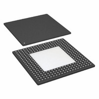
AD8152JBP Analog Devices Inc, AD8152JBP Datasheet - Page 22

AD8152JBP
Manufacturer Part Number
AD8152JBP
Description
Digital Crosspoint 34 x 34 X-Point SW 3.2Gbps 256-Pin SBGA
Manufacturer
Analog Devices Inc
Datasheet
1.AD8152JBPZ.pdf
(32 pages)
Specifications of AD8152JBP
Package
256SBGA
Array Configuration
34x34
Number Of Arrays
1
Maximum Data Rate
3.2 Gbps
Power Supply Type
Single
Minimum Single Supply Voltage
2.25 V
Maximum Single Supply Voltage
3.63 V
Rohs Status
RoHS non-compliant
Function
Crosspoint Switch
Circuit
1 x 34:34
Voltage Supply Source
Single Supply
Voltage - Supply, Single/dual (±)
2.5 V ~ 3.3 V
Current - Supply
32mA
Operating Temperature
0°C ~ 85°C
Mounting Type
Surface Mount
Package / Case
256-BGA Exposed Pad, 256-eBGA, 256-HBGA
Lead Free Status / RoHS Status
Available stocks
Company
Part Number
Manufacturer
Quantity
Price
Company:
Part Number:
AD8152JBP
Manufacturer:
ADI
Quantity:
170
Company:
Part Number:
AD8152JBP
Manufacturer:
Analog Devices Inc
Quantity:
10 000
Company:
Part Number:
AD8152JBPZ
Manufacturer:
ADI
Quantity:
642
Company:
Part Number:
AD8152JBPZ
Manufacturer:
Analog Devices Inc
Quantity:
10 000
AD8152
The variety of supply configurations cause the need for a supply
agile digital control circuitry. This is done by a programmable
logic device (PLD), which provides instructions to the AD8152.
The PLD supply is typically tied with jumpers across the AD8152’s
VCC and VEE supplies (Jumpers J3 and J4). The PLD is addressed
from the PC by way of digital isolators. These couplers isolate
PC levels from the PLD and allow for any level shifting. If
desired, the user can drive the PLD supply separately as long as
the VEE of the AD8152 and the PLD are tied together (remove
Jumper J3 and leave J4 installed). This allows one to measure
the AD8152 only supply current, for example.
Board Construction or Stack-Up
Figure 11 is a picture of AD8152 evaluation board stack-up from
top to bottom. The layer stack-up has been made symmetrical
to avoid board warpage during manufacture. The microstrip
layout and dimensions are shown in Figure 12. The microstrip
trace width was chosen to be 8 mils. This allows relative ease in
routing through the BGA rows that are 50 mils (1.27 mm) apart.
The outer two out of four rows of high speed signals are routed on
top of the PCB, while the inner two rows are via holed to the
board’s opposite side and then routed outward. Wider microstrip
is desirable for reducing eye height loss versus long traces; how-
ever, the routing will be more difficult as the AD8152 is approached.
The wide microstrip would have to be necked down in width in
order to be routed into the BGA. The necking will increase trace
impedance and therefore induce more signal reflection problems.
Figure 13. BGA Corner Capacitor Layout
MICROSTRIP TRACES
Figure 12. Cross-Sectional Layout and Dimensioning (To Scale) of Differential
BGA CORNER OUTLINE
CHIP CAPACITOR
(805) SIZE
VIA HOLE
(GRAY)
–22–
During the layout of the differential microstrip, a software tool
snaps the distance between the two traces to be a constant. If
the distance is not kept constant, impedance variations will
result. These fluctuations can be measured by time domain
reflectometry (TDR).
Bypass Capacitor Layout
The AD8152 8-layer PCB takes advantage of buried interlayer
capacitance. The VEE to VCC planes are placed in the very middle
of the board to make the highest value capacitor. The 4 mil
(0.102 mm) dielectric spacing between VCC/VEE yields 26 nF
of capacitance. Each AD8152 supply pin is directly connected to
its supply plane through a via hole beneath the BGA ball. The
via hole size for a BGA supply pin is slightly bigger than a signal
via. This is to reduce the inductance of the connection, and it
also happens to be a compact layout.
For the chip capacitors, the via holes are placed directly in the
middle of the mounting area and made as large as possible, i.e.,
greater than or equal to 35 mils (0.89 mm). This is to minimize
inductance as much as possible. By minimizing inductance, the
performance of the capacitor or impedance versus frequency
response is not greatly diminished. Note that chip capacitors
will work up to only about 300 MHz.
Figure 14 is an example of a bypass capacitor layout that should
be avoided in any high speed printed circuit board. This layout
connects the chip capacitor mounting pads to small via holes
through a skinny PCB trace. This amounts to four extra inductors
added to the capacitor, two largely from the skinny surface traces
and two from small via holes. Inductance is also variable with
copper thickness and attachment method to power plane. Thermal
relief for soldering purposes also adds unwanted inductance and
should be avoided.
Figure 14. Poor Capacitor Layout
EXTRA ADDED INDUCTANCE
REV. A


