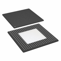
AD8152JBP Analog Devices Inc, AD8152JBP Datasheet - Page 18

AD8152JBP
Manufacturer Part Number
AD8152JBP
Description
Digital Crosspoint 34 x 34 X-Point SW 3.2Gbps 256-Pin SBGA
Manufacturer
Analog Devices Inc
Datasheet
1.AD8152JBPZ.pdf
(32 pages)
Specifications of AD8152JBP
Package
256SBGA
Array Configuration
34x34
Number Of Arrays
1
Maximum Data Rate
3.2 Gbps
Power Supply Type
Single
Minimum Single Supply Voltage
2.25 V
Maximum Single Supply Voltage
3.63 V
Rohs Status
RoHS non-compliant
Function
Crosspoint Switch
Circuit
1 x 34:34
Voltage Supply Source
Single Supply
Voltage - Supply, Single/dual (±)
2.5 V ~ 3.3 V
Current - Supply
32mA
Operating Temperature
0°C ~ 85°C
Mounting Type
Surface Mount
Package / Case
256-BGA Exposed Pad, 256-eBGA, 256-HBGA
Lead Free Status / RoHS Status
Available stocks
Company
Part Number
Manufacturer
Quantity
Price
Company:
Part Number:
AD8152JBP
Manufacturer:
ADI
Quantity:
170
Company:
Part Number:
AD8152JBP
Manufacturer:
Analog Devices Inc
Quantity:
10 000
Company:
Part Number:
AD8152JBPZ
Manufacturer:
ADI
Quantity:
642
Company:
Part Number:
AD8152JBPZ
Manufacturer:
Analog Devices Inc
Quantity:
10 000
AD8152
Input Coupling
One way to simplify the input circuit and make it compatible with
a wide variety of driving devices is to use ac coupling. This has
the effect of isolating the dc common-mode levels of the driver
and the AD8152 input circuitry. For example, the XAUI inter-
connect specification for 10 Gbps Ethernet requires ac coupling
in order to ensure that there are no interactions of dc levels
between the transmitting and receiving devices.
AC coupling requires that the signal patterns have no long-term
dc component, which may occur in any random data stream.
Codes such as 8b/10b, called for in the XAUI specification, are
used in many data communications systems to ensure that the
data pattern is benign in an ac-coupled link. This is accomplished
by run-length limiting (RLL), which sets a maximum for the
number of 1s or 0s that can occur consecutively. In addition,
residual dc components are monitored and modified by keeping
track of the running disparity, excess of 1s versus 0s or vice versa.
For the AD8152 inputs, ac coupling requires a capacitor in series
with each single-ended input signal, as shown in Figure 7. This
should be done in a manner that does not interfere with the high
speed signal integrity of the PC board. The details of this are
covered in the section on board layout guidelines. The two critical
variables are setting the proper voltage for VTTI and selecting
the correct value of coupling capacitors.
On the AD8152 side of the input coupling capacitor, the average
value of the single-ended input voltage will be at the voltage set at
VTTI. The range of allowable voltages is a function of the accept-
able input voltages of the active circuitry of the AD8152 inputs
and the amplitude of the input signal. The operating input range
of the AD8152 extends from VCC + 0.2 V to 0.8 V above VEE.
The total range that will be occupied by the input signal will be
its average value (as established by the voltage applied to VTTI)
plus or minus one half the single-ended swing of the signal. For a
standard 800 mV p-p differential signal, the single-ended swing is
400 mV p-p. Thus, the signal will swing ± 200 mV about the
average value equal to VTTI.
Figure 7. AC-Coupling Input Signal from AD8152
C
C
INP
INN
INXXP
INXXN
50
VTTI
50
VCC
VEE
–18–
If VTTI is set equal to VCC, then the single-ended signal will
just meet the specifications where its highest excursion will be
0.2 V higher than VCC. The lowest level to set VTTI is 0.8 V
above VEE. This will cause the negative signal excursions to stay
within the operating range.
With ac-coupled inputs, there is no power consumption advan-
tage associated with varying VTTI. As a practical matter, it
might be desirable to set VTTI at the same voltage as VTTO so
that only one supply is necessary. Refer to the VTTO section for
more information.
Output Coupling
Each single-ended output of the AD8152 has a termination
resistor that ties to a common point called VTTO. When VTTO
is varied, it will change the common-mode levels of the outputs
and the power dissipation of the output stages when they are
enabled.
The individual output currents are programmable. Varying this
current will change the lower level of the output voltage (and thus
the peak-to-peak swing) and also change the power dissipation in
the output stages. To obtain a standard 800 mV p-p differential
output (single-ended = 400 mV p-p), the output current should
be programmed to 16 mA. With an effective termination resis-
tance of 25 W, this will generate the proper differential voltage.
If the AD8152 drives another device that is ac-coupled, there is no
interaction of the dc levels on each side of the coupling capacitors
(see Figure 8). The dc levels for the AD8152 can be calculated
independent of the levels of the device that is driven.
The upper allowable setting for VTTO is 0.2 V higher than VCC.
The signals will be pulled up to this level at their highest excursion.
However at this setting, the power dissipation will be a maximum.
To save power, VTTO can be lowered. The lowest level for
VTTO will be determined by the lowest output level allowable
(V
at any time should not go lower than 1.0 V below VCC. If the
single-ended swing of an output is 400 mV p-p, then the lowest
that VTTO can go is 0.6 V below VCC. For more information
on V
VCC
VEE
OL
Figure 8. AC-Coupling Output Signal from AD8152
) by the AD8152 output when it is logically low. The output
OL
AD8152
, see TPC 17.
50
VTTO
VEE
I = 2mA
50
(CODE) + 2mA
OUTXXP
OUTXXN
DRIVEN DEVICE
VTT
VEE
REV. A
VCC


