AD8152JBP Analog Devices Inc, AD8152JBP Datasheet - Page 14
AD8152JBP
Manufacturer Part Number
AD8152JBP
Description
Digital Crosspoint 34 x 34 X-Point SW 3.2Gbps 256-Pin SBGA
Manufacturer
Analog Devices Inc
Datasheet
1.AD8152JBPZ.pdf
(32 pages)
Specifications of AD8152JBP
Package
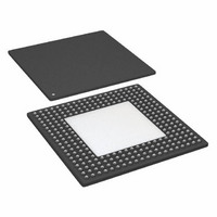
256SBGA
Array Configuration
34x34
Number Of Arrays
1
Maximum Data Rate
3.2 Gbps
Power Supply Type
Single
Minimum Single Supply Voltage
2.25 V
Maximum Single Supply Voltage
3.63 V
Rohs Status
RoHS non-compliant
Function
Crosspoint Switch
Circuit
1 x 34:34
Voltage Supply Source
Single Supply
Voltage - Supply, Single/dual (±)
2.5 V ~ 3.3 V
Current - Supply
32mA
Operating Temperature
0°C ~ 85°C
Mounting Type
Surface Mount
Package / Case
256-BGA Exposed Pad, 256-eBGA, 256-HBGA
Lead Free Status / RoHS Status
Available stocks
Company
Part Number
Manufacturer
Quantity
Price
Company:

Part Number:
AD8152JBP
Manufacturer:
ADI
Quantity:
170
Company:
Part Number:
AD8152JBP
Manufacturer:
Analog Devices Inc
Quantity:
10 000
Company:
Part Number:
AD8152JBPZ
Manufacturer:
ADI
Quantity:
642
Company:
Part Number:
AD8152JBPZ
Manufacturer:
Analog Devices Inc
Quantity:
10 000


AD8152
Symbol
t
t
t
t
t
t
t
Symbol
t
t
t
t
t
t
CSW
ASW
DSW
CHW
AHW
DHW
WP
CSU
CHU
UOE
UOT
UOD
UW
Setup Time
Hold Time
Output Enable Times
Output Toggle Times
Output Disable Times
Width of Update Pulse
Setup Time
Hold Time
Width of Write Enable Pulse
Parameter
A[6:0]INPUTS
D[5:0]INPUTS
OUT[0:33][N:P]
OUT[0:33][N:P]
OUT[0:33][N:P]
Parameter
Chip Select to Write Enable
Address to Write Enable
Data to Write Enable
Chip Select from Write Enable
Address from Write Enable
Data from Write Enable
DISABLING
ENABLING
OUTPUTS
OUTPUTS
OUTPUTS
CS
WE
Chip Select to Update
Chip Select from Update
Update to Output Enable
Update to Output Reprogram
Update to Output Disabled
UPDATE
TOGGLE
CS
Figure 3b. Second Rank Update Cycle
Table VI. Second Rank Update Cycle
Figure 3a. First Rank Write Cycle
Table V. First Rank Write Cycle
DATA FROM RANK 2
t
CSU
t
CSW
PREVIOUS RANK 2 DATA
t
UOE
t
ASW
t
UOD
–14–
t
UOT
DATA FROM RANK 1
t
WP
t
UW
t
DSW
Conditions
T
VCC = 3.3 V
Conditions
T
VCC = 3.3 V
A
A
= 25 C
= 25 C
t
AHW
DATA FROM RANK 1
t
DHW
t
t
AHW
CHW
t
CHU
Min
0
0
1
0
0
0
10
Min
0
0
10
Typ
Typ
25
25
25
Max
Max
45
45
45
Unit
ns
ns
ns
ns
ns
ns
ns
Unit
ns
ns
ns
ns
ns
ns
REV. A
Related parts for AD8152JBP
Image
Part Number
Description
Manufacturer
Datasheet
Request
R

Part Number:
Description:
±1.7g Dual-Axis IMEMS Accelerometer Evaluation Board
Manufacturer:
Analog Devices Inc
Datasheet:

Part Number:
Description:
Inertial Sensor Evaluation System
Manufacturer:
Analog Devices Inc
Datasheet:
Part Number:
Description:
Manufacturer:
Analog Devices Inc
Datasheet:
Part Number:
Description:
Manufacturer:
Analog Devices Inc
Datasheet:
Part Number:
Description:
Manufacturer:
Analog Devices Inc
Datasheet:
Part Number:
Description:
Manufacturer:
Analog Devices Inc
Datasheet:
Part Number:
Description:
Manufacturer:
Analog Devices Inc
Datasheet:
Part Number:
Description:
Manufacturer:
Analog Devices Inc
Datasheet:
Part Number:
Description:
Manufacturer:
Analog Devices Inc
Datasheet:
Part Number:
Description:
Manufacturer:
Analog Devices Inc
Datasheet:
Part Number:
Description:
Manufacturer:
Analog Devices Inc
Datasheet:
Part Number:
Description:
Manufacturer:
Analog Devices Inc
Datasheet:
Part Number:
Description:
Manufacturer:
Analog Devices Inc
Datasheet: