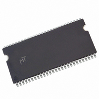
MT48LC4M16A2P-6:G Micron Technology Inc, MT48LC4M16A2P-6:G Datasheet - Page 38

MT48LC4M16A2P-6:G
Manufacturer Part Number
MT48LC4M16A2P-6:G
Description
DRAM Chip SDRAM 64M-Bit 4Mx16 3.3V 54-Pin TSOP-II Tray
Manufacturer
Micron Technology Inc
Type
SDRAMr
Datasheet
1.MT48LC4M16A2P-75G_TR.pdf
(72 pages)
Specifications of MT48LC4M16A2P-6:G
Density
64 Mb
Maximum Clock Rate
166 MHz
Package
54TSOP-II
Address Bus Width
14 Bit
Operating Supply Voltage
3.3 V
Maximum Random Access Time
5.5 ns
Operating Temperature
0 to 70 °C
Format - Memory
RAM
Memory Type
SDRAM
Memory Size
64M (4M x 16)
Speed
167MHz
Interface
Parallel
Voltage - Supply
3 V ~ 3.6 V
Package / Case
54-TSOP II
Organization
4Mx16
Address Bus
14b
Access Time (max)
5.5ns
Operating Supply Voltage (typ)
3.3V
Package Type
TSOP-II
Operating Temp Range
0C to 70C
Operating Supply Voltage (max)
3.6V
Operating Supply Voltage (min)
3V
Supply Current
180mA
Pin Count
54
Mounting
Surface Mount
Operating Temperature Classification
Commercial
Lead Free Status / RoHS Status
Lead free / RoHS Compliant
Available stocks
Company
Part Number
Manufacturer
Quantity
Price
Company:
Part Number:
MT48LC4M16A2P-6:G
Manufacturer:
MICRON
Quantity:
3 000
Figure 30:
Figure 31:
PDF: 09005aef80725c0b/Source: 09005aef806fc13c
64MSDRAM_2.fm - Rev. N 12/08 EN
READ With Auto Precharge Interrupted by a WRITE
WRITE With Auto Precharge Interrupted by a READ
Notes:
Notes:
1. DQM is HIGH at T2 to prevent D
1. DQM is LOW.
Internal
States
Internal
States
COMMAND
COMMAND
ADDRESS
ADDRESS
BANK m
BANK m
BANK n
BANK n
DQM
CLK
CLK
DQ
DQ
1
Active
Page
READ - AP
BANK n,
BANK n
Page Active
COL a
T0
T0
NOP
READ with Burst of 4
CAS Latency = 3 (BANK n)
WRITE - AP
BANK n,
Page Active
Page Active
BANK n
COL a
T1
NOP
T1
D
a
IN
38
WRITE with Burst of 4
OUT
T2
T2
a +1 from contending with D
a + 1
NOP
NOP
D
IN
Micron Technology, Inc., reserves the right to change products or specifications without notice.
BANK m,
READ - AP
T3
T3
COL d
BANK m
D
NOP
OUT
a
Interrupt Burst, Write-Back
t
CAS Latency = 3 (BANK m)
WR - BANK n
READ with Burst of 4
BANK m,
WRITE - AP
TRANSITIONING DATA
COL d
TRANSITIONING DATA
BANK m
T4
T4
D
NOP
d
IN
Interrupt Burst, Precharge
WRITE with Burst of 4
64Mb: x4, x8, x16 SDRAM
T5
T5
d + 1
NOP
D
NOP
IN
Precharge
t
©2000 Micron Technology, Inc. All rights reserved.
RP - BANK n
t
IN
RP - BANK n
d at T4.
T6
T6
d + 2
NOP
D
D
NOP
IN
OUT
d
DON’T CARE
Commands
DON’T CARE
T7
t WR - BANK m
T7
d + 3
d + 1
NOP
D
D
NOP
IN
t RP - BANK m
OUT
Write-Back
Idle


