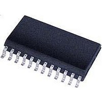
CS5461A-ISZR Cirrus Logic Inc, CS5461A-ISZR Datasheet - Page 15

CS5461A-ISZR
Manufacturer Part Number
CS5461A-ISZR
Description
IC Sngl-Phs Bi-Directional Power/Energy
Manufacturer
Cirrus Logic Inc
Datasheet
1.CS5461A-ISZ.pdf
(44 pages)
Specifications of CS5461A-ISZR
Input Impedance
30 KOhm
Measurement Error
0.1%
Voltage - I/o High
0.8V
Voltage - I/o Low
0.2V
Current - Supply
2.9mA
Voltage - Supply
4.75 V ~ 5.25 V
Operating Temperature
-40°C ~ 85°C
Mounting Type
Surface Mount
Package / Case
24-SSOP
Meter Type
Single Phase
Lead Free Status / RoHS Status
Lead free / RoHS Compliant
For Use With
598-1552 - BOARD EVAL & SOFTWARE CS5461A
Lead Free Status / Rohs Status
Lead free / RoHS Compliant
Available stocks
Company
Part Number
Manufacturer
Quantity
Price
Part Number:
CS5461A-ISZR
Manufacturer:
CIRRUS
Quantity:
20 000
5. FUNCTIONAL DESCRIPTION
5.1 Analog Inputs
The CS5461A is equipped with two fully differential in-
put channels. The inputs VIN± and IIN± are designated
as the voltage and current channel inputs, respectively.
The full-scale differential input voltage for the current
and voltage channel is ±250 mV
5.1.1 Voltage Channel
The output of the line-voltage resistive divider or trans-
former is connected to the VIN+ and VIN- input pins of
the CS5461A. The voltage channel is equipped with a
10x, fixed-gain amplifier. The full-scale signal level that
can be applied to the voltage channel is ±250 mV. If the
input signal is a sine wave the maximum RMS voltage
at a gain 10x is:
which is approximately 70.7% of maximum peak volt-
age. The voltage channel is also equipped with a Volt-
age
programmable gain of up to 4x.
5.1.2 Current Channel
The output of the current-sense resistor or transformer
is connected to the IIN+ and IIN- input pins of the
CS5461A. To accommodate different current-sensing
elements, the current channel incorporates a Program-
mable Gain Amplifier (PGA) with two programmable in-
put gains. Configuration Register bit Igain (See Table 1)
defines the two gain selections and corresponding max-
imum input-signal level.
For example, if Igain=0, the current channel’s PGA gain
is set to 10x. If the input signals are pure sinusoids with
zero phase shift, the maximum peak differential signal
on the current or voltage channel is ±250 mV
put-signal levels are approximately 70.7% of maximum
peak voltage producing a full-scale energy pulse regis-
tration equal to 50% of absolute maximum energy pulse
registration. This will be discussed further in
Energy Pulse Output
The Current Gain Register also allows for an additional
programmable gain of up to 4x. If an additional gain is
DS661F2
Table 1. Current Channel PGA Configuration
Gain
Igain
Register,
0
1
250mV P
-------------------- -
2
Maximum Input Range
on page 16.
±250 mV
±50 mV
≅
allowing
176.78mV RMS
P
.
for
10x
50x
an
Section 5.4
additional
P
. The in-
applied to the voltage and/or current channel, the maxi-
mum input range should be adjusted accordingly.
5.2 High-pass Filters
By removing the offset from either channel, no error
component will be generated at DC when computing the
active power. By removing the offset from both chan-
nels, no error component will be generated at DC when
computing V
tion Register bits VHPF and IHPF activate the HPF in
the voltage and current channel respectively.
5.3 Performing Measurements
The CS5461A performs measurements of instanta-
neous voltage (V
stantaneous power (P
of
where K is the clock divider setting in the Configuration
Register.
The RMS voltage (V
tive power (P
neous samples of V
the value in the Cycle Count Register (N) and is referred
to as a “computation cycle”. The apparent power (S) is
the product of V
derived from the master clock (MCLK), with frequency:
Under default conditions & with K = 1, N = 4000, and
MCLK = 4.096 MHz – the OWR = 4000 Hz and the
Computation Cycle = 1 Hz.
All measurements are available as a percentage of full
scale. The format for signed registers is a two’s comple-
ment, normalized value between -1 and +1. The format
for unsigned registers is a normalized value between 0
and 1. A register value of
represents the maximum possible value.
At each instantaneous measurement, the CRDY bit will
be set (logic 1) in the Status Register, and the INT pin
will become active if the CRDY bit is unmasked in the
Mask Register. At the end of each computation cycle,
the DRDY bit will be set in the Status Register, and the
RMS
Active
Computation Cycle
, I
RMS
n
(
----------------------- -
2
RMS
) and current (I
OWR
23
) are computed using N instanta-
2
n
RMS
23
, I
and I
–
n
, and apparent power. Configura-
n
) at an Output Word Rate (OWR)
1
and P
)
), RMS current (I
=
=
RMS
(
---------------------------- -
MCLK K
0.99999988
1024
n
. A computation cycle is
respectively, where N is
=
⁄
n
OWR
-------------- -
), and calculates in-
)
N
CS5461A
RMS
), and ac-
15


