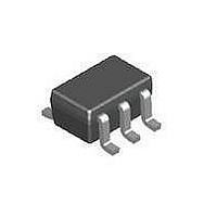
MUN5312DW1T2 ON Semiconductor, MUN5312DW1T2 Datasheet - Page 3

MUN5312DW1T2
Manufacturer Part Number
MUN5312DW1T2
Description
Digital Transistors 100mA Complementary
Manufacturer
ON Semiconductor
Datasheet
1.MUN5312DW1T2.pdf
(34 pages)
Specifications of MUN5312DW1T2
Configuration
Dual
Transistor Polarity
NPN/PNP
Typical Input Resistor
22 KOhm
Typical Resistor Ratio
1
Mounting Style
SMD/SMT
Package / Case
SC-88
Collector- Emitter Voltage Vceo Max
50 V
Continuous Collector Current
0.1 A
Peak Dc Collector Current
100 mA
Power Dissipation
187 mW
Maximum Operating Temperature
+ 150 C
Minimum Operating Temperature
- 55 C
Lead Free Status / RoHS Status
Lead free / RoHS Compliant
Available stocks
Company
Part Number
Manufacturer
Quantity
Price
Part Number:
MUN5312DW1T2
Manufacturer:
ON/安森美
Quantity:
20 000
Company:
Part Number:
MUN5312DW1T2G
Manufacturer:
ON
Quantity:
30 000
3. Pulse Test: Pulse Width < 300 ms, Duty Cycle < 2.0%
ELECTRICAL CHARACTERISTICS
(T
OFF CHARACTERISTICS
Collector-Base Cutoff Current (V
Collector-Emitter Cutoff Current (V
Emitter-Base Cutoff Current
Collector-Base Breakdown Voltage (I
Collector-Emitter Breakdown Voltage (Note 3) (I
A
(V
= 25°C unless otherwise noted, common for Q
EB
= 6.0 V, I
C
= 0)
Characteristic
CB
CE
= 50 V, I
C
= 50 V, I
= 10 mA, I
E
= 0)
B
= 0)
C
MUN5311DW1T1G
MUN5312DW1T1G
MUN5313DW1T1G
MUN5314DW1T1G
MUN5315DW1T1G
MUN5316DW1T1G
MUN5330DW1T1G
MUN5331DW1T1
MUN5332DW1T1G
MUN5333DW1T1
MUN5334DW1T1G
MUN5335DW1T1G
E
1
= 2.0 mA, I
= 0)
and Q
http://onsemi.com
2
, − minus sign for Q
B
= 0)
G
G
3
V
V
Symbol
(BR)CBO
(BR)CEO
I
I
I
CBO
CEO
EBO
1
(PNP) omitted)
Min
50
50
−
−
−
−
−
−
−
−
−
−
−
−
−
−
Typ
−
−
−
−
−
−
−
−
−
−
−
−
−
−
−
−
Max
0.18
0.13
100
500
0.5
0.2
0.1
0.2
0.9
1.9
4.3
2.3
1.5
0.2
−
−
mAdc
nAdc
nAdc
Unit
Vdc
Vdc


