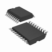
RFHCS362GT-I/SO Microchip Technology, RFHCS362GT-I/SO Datasheet - Page 34

RFHCS362GT-I/SO
Manufacturer Part Number
RFHCS362GT-I/SO
Description
IC CODE HOPPNG ENCDR W/RF 18SOIC
Manufacturer
Microchip Technology
Datasheet
1.RFHCS362F-ISS.pdf
(60 pages)
Specifications of RFHCS362GT-I/SO
Frequency
310MHz ~ 440MHz
Applications
Automotive, Building Access, Garage Openers
Modulation Or Protocol
ASK, FSK
Data Rate - Maximum
3.3 kbps
Power - Output
-12dBm ~ 2dBm
Current - Transmitting
11.5mA
Data Interface
PCB, Surface Mount
Antenna Connector
PCB, Surface Mount
Voltage - Supply
2.2 V ~ 5.5 V
Operating Temperature
-40°C ~ 85°C
Package / Case
18-SOIC (0.300", 7.50mm Width)
Lead Free Status / RoHS Status
Lead free / RoHS Compliant
Features
-
Memory Size
-
rfHCS362G/362F
6.6
The PLL output feeds the power amplifier (PA). The
open-collector differential output (ANT1, ANT2) can be
used to drive a loop antenna directly or converted to
single-ended output via an impenance matching net-
work or balanced-to-unbalanced (balun) transformer.
Pins ANT1 and ANT2 are open-collector outputs and
must be pulled-up to V
The differential output of the PA should be matched to
an impedance of 800 to 1000
impedance may cause excessive spurious and har-
monic emissions. For more information see Application
Note AN831, Matching Small Loop Antennas to rfPIC
Devices.
The transmit output power can be adjusted in six dis-
crete steps from +2 dBm to -12 dBm by varying the volt-
age (V
example voltage divider network for ASK operation and
Figure 6-6 for FSK operation.
For FSK operation, the PS/DATA
a Power Select (PS) pin. An internal 20
source pushes current through the PS/DATA
resulting in a voltage drop across resistor R2 at the V
level selected for transmitter output power. V
the PA bias current. Higher transmit power will draw
higher current.
For ASK operation, the function of the PS/DATA
is to turn the Power Amplifier (PA) on and off. Resistors
R1 and R2 form a voltage divider network to apply volt-
age V
maximum transmitter output is desired, the output of a
GP0 pin can be connected directly to PS/DATA
Table 6-6 lists typical values for R1 and R2 for both the
ASK and FSK modes.
TABLE 6-6:
DS41189A-page 34
Note 1: Standard Operating Conditions (unless otherwise stated) T
Output Power
Transmitter
PS
PS
(dBm)
) at the PS/DATA
Power Amplifier
-10
-12
-60
2: V
3: The Power Select circuitry contains an internal 20 A current source. To ensure that the transmitter output
for the selected transmitter output power. If
+2
-1
-4
-7
V
power is at the minimum when transmitting a DATA
that the voltage drop across it is less than 0.1 volts.
DDRF
PS
is actual voltage on PS/DATA
POWER SELECT
= 3V, f
DDRF
Operating Current
ASK
TRANSMIT
Transmitter
through the load.
pin. Figure 6-5 shows an
(mA)
11.5
<4.8
8.6
7.3
6.2
5.3
4.8
ASK
Failure to match the
= 433.92 MHz
pin only serves as
(1)
PS
A current
ASK
Power Select (PS)
ASK
ASK
ASK
selects
Voltage V
.
Preliminary
pin.
pin
pin
(Volts)
PS
<0.1
1.2
0.9
0.7
0.5
0.3
2.0
(2)
PS
.
FIGURE 6-5:
FIGURE 6-6:
ASK
Note: PS/DATA
DATA IN
= 0 (V
Make sure external circuitry on PS/DATA
does not conflict by driving the pin high. The
encoder DATA output works because it is low if
RFEN
A
R1 ( )
OPEN
2400
6800
15K
= 25°C, RF
11K
24K
43K
SSRF
OUT
), select the value of resistor R2 such
ASK
is low
R1
EXAMPLE FSK POWER
EXAMPLE ASK POWER
SELECT CIRCUIT
SELECT CIRCUIT
ASK
is driven low when RFEN
EN
PS/DATA
R2
R2 ( )
= 1,
V
PS
2002 Microchip Technology Inc.
4700
4700
4700
4700
4700
4700
4700
ASK
PS/DATA
R2
(3)
V
PS
rfHCS362G/362F
ASK
20
A
rfHCS362G/362F
To power
select
circuitry
20
R2 ( )
4700
FSK
A
56K
47K
39K
27K
15K
75K
To power
select
circuitry
IN
= 0.
ASK


