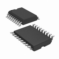
RFHCS362GT-I/SO Microchip Technology, RFHCS362GT-I/SO Datasheet - Page 27

RFHCS362GT-I/SO
Manufacturer Part Number
RFHCS362GT-I/SO
Description
IC CODE HOPPNG ENCDR W/RF 18SOIC
Manufacturer
Microchip Technology
Datasheet
1.RFHCS362F-ISS.pdf
(60 pages)
Specifications of RFHCS362GT-I/SO
Frequency
310MHz ~ 440MHz
Applications
Automotive, Building Access, Garage Openers
Modulation Or Protocol
ASK, FSK
Data Rate - Maximum
3.3 kbps
Power - Output
-12dBm ~ 2dBm
Current - Transmitting
11.5mA
Data Interface
PCB, Surface Mount
Antenna Connector
PCB, Surface Mount
Voltage - Supply
2.2 V ~ 5.5 V
Operating Temperature
-40°C ~ 85°C
Package / Case
18-SOIC (0.300", 7.50mm Width)
Lead Free Status / RoHS Status
Lead free / RoHS Compliant
Features
-
Memory Size
-
5.0
When using the rfHCS362G/362F in a system, the user
will have to program some parameters into the device,
including the serial number and the secret key before it
can be used. The programming cycle allows the user to
input all 288 bits in a serial data stream, which are then
stored internally in EEPROM. Programming will be
initiated by forcing the DATA line HIGH, after the S2 line
has been held HIGH for the appropriate length of time
(Table 10-3 and Figure 5-1). After the Program mode is
entered, a delay must be provided to the device for the
automatic bulk write cycle to complete. This will write all
locations in the EEPROM to an all zeros pattern includ-
ing the OSC calibration bits.
The device can then be programmed by clocking in 16
bits at a time, using S2 as the clock line and DATA as
the data in-line. After each 16-bit word is loaded, a pro-
gramming delay is required for the internal program
FIGURE 5-1:
FIGURE 5-2:
S2 (S3)
S2 (S3)
(Clock)
(Clock)
Note 1: Unused button inputs to be held to ground during the entire programming sequence.
(Data)
DATA
DATA
(Data)
2002 Microchip Technology Inc.
Note: If a Verify operation is to be done, then it must immediately follow the Program cycle.
End of Programming Cycle
2: The V
PROGRAMMING THE
rfHCS362G/362F
Enter Program
Bit286
T
PS
Mode
DD
Bit287
T
PH
pin must be taken to ground after a Program/Verify cycle.
1
PROGRAMMING WAVEFORMS
T
VERIFY WAVEFORMS
PH
T
2
WC
T
PBW
T
Bit 0
Beginning of Verify Cycle
CLKH
Bit 0
T
CLKL
Bit 1
Bit 1 Bit 2
T
Bit 2
DS
T
Preliminary
DV
Repeat for each word (18 times)
T
Bit 3
DH
Data for Word 0 (KEY_0)
Data from Word 0
Bit 3
cycle to complete. This delay can take up to Twc. At the
end of the programming cycle, the device can be veri-
fied (Figure 5-2) by reading back the EEPROM. Read-
ing is done by clocking the S2 line and reading the data
bits on DATA. For security reasons, it is not possible to
execute a Verify function without first programming the
EEPROM. A Verify operation can only be done
once, immediately following the Program cycle.
Bit 14
Note:
Bit 14
Bit 15
rfHCS362G/362F
To ensure that the device does not
accidentally enter Programming mode,
DATA should never be pulled high by
the circuit connected to it. Special care
should be taken when driving circuits
other than the RFEN
Bit 15
T
WC
Bit 16 Bit 17
IN
.
Bit 16
DS41189A-page 27
Data for Word 1
Bit286 Bit287
Bit 17


