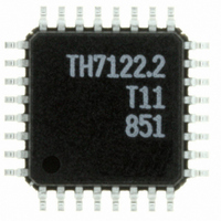
TH7122ENE Melexis Inc, TH7122ENE Datasheet - Page 19

TH7122ENE
Manufacturer Part Number
TH7122ENE
Description
IC TXRX 930MHZ FSK/FM/ASK 32LQFP
Manufacturer
Melexis Inc
Specifications of TH7122ENE
Frequency
300MHz ~ 930MHz
Data Rate - Maximum
115Kbps
Modulation Or Protocol
ASK, FM, FSK
Applications
Alarm and Security Systems, RKE, TPMS
Power - Output
-10dBm ~ 11dBm
Sensitivity
-105dBm
Voltage - Supply
2.2 V ~ 5.5 V
Current - Receiving
14mA
Current - Transmitting
23mA @ 10dBm
Data Interface
PCB, Surface Mount
Antenna Connector
PCB, Surface Mount
Operating Temperature
-40°C ~ 85°C
Package / Case
32-LQFP
Transmitting Current
12mA
Data Rate
115Kbps
Frequency Range
300MHz To 930MHz
Modulation Type
AM, FM, FSK
Sensitivity Dbm
-105dBm
Rf Ic Case Style
LQFP
No. Of Pins
32
Supply Voltage
RoHS Compliant
Output Power
10dBm
Rohs Compliant
Yes
Lead Free Status / RoHS Status
Lead free / RoHS Compliant
Memory Size
-
Lead Free Status / RoHS Status
Lead free / RoHS Compliant
Other names
TH7122.3
TH7122ENETR
TH7122ENETR
Available stocks
Company
Part Number
Manufacturer
Quantity
Price
4.1.3
4.1.4
4.2
The transceiver can also be used in programmable user mode. After power-up the first logic change at pin
FS0/SDEN enters into this mode. Now full programmability can be achieved via the Serial Control Interface
(SCI).
4.2.1
A 3-wire (SCLK, SDTA, SDEN) Serial Control Interface (SCI) is used to program the transceiver in program-
mable user mode. At each rising edge of the SCLK signal, the logic value on the SDTA pin is written into a
24-bit shift register. The data stored in the shift register are loaded into one of the 4 appropriate latches on
the rising edge of SDEN. The control words are 24 bits lengths: 2 address bits and 22 data bits. The first two
bits (bit 23 and 22) are latch address bits. As additional leading bits are ignored, only the least significant 24
bits are serial-clocked into the shift register. The first incoming bit is the most significant bit (MSB). To
program the transceiver in multi-channel application, four 24-bit words may be sent: A-word, B-word, C-word
and D-word. If individual bits within a word have to be changed, then it is sufficient to program only the
appropriate 24-bit word. The serial data input timing and the structure of the control words are illustrated in
Fig. 12 and 13.
39010 07122
Rev. 010
Programmable User Mode Operation
Modulation Type
LNA Gain Mode
Serial Control Interface Description
Modulation type
SDTA
SCLK
SDEN
GAIN_LNA
ASK / FSK
LNA gain
SHIFT REGISTER
ADDR DECODER
24-BIT
2
Fig. 12: SCI Block Diagram
Page 19 of 44
‘
‘
‘
‘
00
01
10
11
22
’
’
’
’
ASK
high
0
0
22
22
22
22
B - LATCH
C - LATCH
D - LATCH
A - LATCH
FSK/FM/ASK Transceiver
22
22
22
22
27 to 930MHz
FSK
TH7122
low
A-word
B-word
C-word
D-word
1
1
Data Sheet
Feb/09


