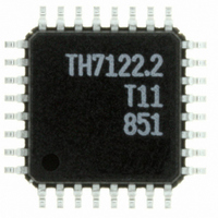
TH7122ENE Melexis Inc, TH7122ENE Datasheet - Page 10

TH7122ENE
Manufacturer Part Number
TH7122ENE
Description
IC TXRX 930MHZ FSK/FM/ASK 32LQFP
Manufacturer
Melexis Inc
Specifications of TH7122ENE
Frequency
300MHz ~ 930MHz
Data Rate - Maximum
115Kbps
Modulation Or Protocol
ASK, FM, FSK
Applications
Alarm and Security Systems, RKE, TPMS
Power - Output
-10dBm ~ 11dBm
Sensitivity
-105dBm
Voltage - Supply
2.2 V ~ 5.5 V
Current - Receiving
14mA
Current - Transmitting
23mA @ 10dBm
Data Interface
PCB, Surface Mount
Antenna Connector
PCB, Surface Mount
Operating Temperature
-40°C ~ 85°C
Package / Case
32-LQFP
Transmitting Current
12mA
Data Rate
115Kbps
Frequency Range
300MHz To 930MHz
Modulation Type
AM, FM, FSK
Sensitivity Dbm
-105dBm
Rf Ic Case Style
LQFP
No. Of Pins
32
Supply Voltage
RoHS Compliant
Output Power
10dBm
Rohs Compliant
Yes
Lead Free Status / RoHS Status
Lead free / RoHS Compliant
Memory Size
-
Lead Free Status / RoHS Status
Lead free / RoHS Compliant
Other names
TH7122.3
TH7122ENETR
TH7122ENETR
Available stocks
Company
Part Number
Manufacturer
Quantity
Price
3
3.1
The TH7122 contains an integer-N PLL frequency synthesizer. A PLL circuit performs the frequency synthe-
sis via a feedback mechanism. The output frequency f
detector comparison frequency f
f
locked state it must be equal to the desired output frequency, divided by the feedback divider ratio N.
Fig. 2:
The output frequency of the synthesizer f
reference divider. The only constraint for the frequency output of the system is that the minimum frequency
resolution, or the channel spacing, must be equal to the PFD frequency f
frequency f
When the PLL is unlocked (e.g. during power up or during reprogramming of a new feedback divider ratio N),
the phase-frequency detector PFD and the charge pump create an error signal proportional to the phase
difference of the two input signals. This error signal is low-pass filtered through the external loop filter and
input to the VCO to control its frequency. A very low frequency resolution increases the settling time of the
PLL and reduces the ability to cancel out VCO perturbations, because the loop filter is updated every 1/f
After the PLL has locked, the VCO frequency is given by the following equation:
There are four registers available to set the VCO frequencies in receive (registers RR and NR) and in trans-
mit mode (registers RT and NT). These registers can be programmed using the Serial Control Interface in
Programmable User Mode (PUM). In case of Stand-alone User Mode (SUM), the registers are set fixed val-
ues (refer to para. 4.1.1).
The VCO frequency is equal to the carrier frequency in transmit mode. While in receive mode the VCO
frequency is offset by the intermediate frequency IF. This is because of the super-heterodyne nature of the
receive part.
39010 07122
Rev. 010
RO
of a crystal oscillator. The phase detector utilizes this signal as a reference to tune the VCO and in the
Reference
Oscillator
Functional Description
PLL Frequency Synthesizer
Integer-N PLL Frequency Synthesizer Topology
RO
and the reference divider factor R:
f
RO
Reference
Divider
f
f
R
VCO
Phase-frequency
f
=
R
R
f
.This reference frequency f
=
R
RO
Detector
N
.
f
⋅
N
f
VCO
R
RO
=
can be selected by programming the feedback divider and the
Page 10 of 44
N
Charge
⋅
Pump
f
R
.
VCO
is generated as an integer multiple of the phase
R
is generated by dividing the output frequency
Feedback
Divider
VCC
LF
FSK/FM/ASK Transceiver
R
, which is given by the reference
Loop Filter
Voltage Controlled
External
Oscillator
(1)
(2)
27 to 930MHz
TH7122
f
Data Sheet
VCO
Feb/09
R
.


