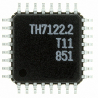
TH7122ENE Melexis Inc, TH7122ENE Datasheet - Page 13

TH7122ENE
Manufacturer Part Number
TH7122ENE
Description
IC TXRX 930MHZ FSK/FM/ASK 32LQFP
Manufacturer
Melexis Inc
Specifications of TH7122ENE
Frequency
300MHz ~ 930MHz
Data Rate - Maximum
115Kbps
Modulation Or Protocol
ASK, FM, FSK
Applications
Alarm and Security Systems, RKE, TPMS
Power - Output
-10dBm ~ 11dBm
Sensitivity
-105dBm
Voltage - Supply
2.2 V ~ 5.5 V
Current - Receiving
14mA
Current - Transmitting
23mA @ 10dBm
Data Interface
PCB, Surface Mount
Antenna Connector
PCB, Surface Mount
Operating Temperature
-40°C ~ 85°C
Package / Case
32-LQFP
Transmitting Current
12mA
Data Rate
115Kbps
Frequency Range
300MHz To 930MHz
Modulation Type
AM, FM, FSK
Sensitivity Dbm
-105dBm
Rf Ic Case Style
LQFP
No. Of Pins
32
Supply Voltage
RoHS Compliant
Output Power
10dBm
Rohs Compliant
Yes
Lead Free Status / RoHS Status
Lead free / RoHS Compliant
Memory Size
-
Lead Free Status / RoHS Status
Lead free / RoHS Compliant
Other names
TH7122.3
TH7122ENETR
TH7122ENETR
Available stocks
Company
Part Number
Manufacturer
Quantity
Price
The CNT_ER supervises the unlock condition. If Up and Down are consecutive, the counter CNT_ER will be
reloaded permanently and its CARRY will not be set, otherwise the counter level of CNT_ER will be reduced
by the reference oscillator clock (1/f
during Up and Down signals can be non-consecutive without loosing the locked state.
The transceiver offers two ways of analyzing the locked state. If the register LOCKMODE is set to ‘0’, only
one occurrence of the locked state condition is needed to remain LD = 1 during the whole active mode, oth-
erwise the state of the PLL will be observed permanently.
3.1.7
The transceiver provides a LC-based voltage-controlled oscillator with an
external inductance element connected between VCC and pin TNK_LO.
An internal varactor diode in series with a fixed capacitor forms the vari-
able part of the oscillator tank. The oscillation frequency is adjusted by
the DC-voltage at pin LF. The tuning sensitivity of the VCO is approxi-
mately 20MHz/V for 433MHz operations and 40MHz/V at 868MHz. Since
the internal varactor is connected to VCC, a lower voltage on pin LF
causes the capacitance to decrease and the VCO frequency to increase.
For this reason the phase detector polarity should be negative (PFDPOL
= 0). If the operation frequency is below 300MHz, an external varactor
diode between pin TNK_LO and VCC_PLL is necessary. The corre-
sponding application schematic is shown in section 8. The VCO current
VCOCUR can be adjusted via serial control interface in order to ensure
stable oscillations over the whole frequency range. For lowest LO emis-
sion in receive mode, VCOCUR should be set to the lowest value.
3.1.8
Since the loop filter has a strong impact on the function of the PLL, it
must be chosen carefully. For FSK operation the bandwidth of the loop
filter must be selected wide enough for a fast relock of the PLL during
crystal pulling. The bandwidth must of course also be larger than the data
rate. In case of ASK or OOK the bandwidth should be extended even
further to allow the PLL to cancel out VCO perturbations that might be
caused by the PA on/off keying. The suggested filter topology is shown in
Fig. 6. The dimensions of the loop filter elements can be derived using
well known formulas in application notes and other reference literature.
3.2
The RF front-end of the receiver part is a super-heterodyne configuration that converts the input radio-
frequency (RF) signal into an intermediate frequency (IF) signal. The most commonly used IF is 10.7 MHz,
but IFs in the range of 0.4 to 22 MHz can also be used. According to the block diagram, the front-end con-
sists of a LNA, a Mixer and an IF limiting amplifier with received signal strength indicator (RSSI). The local
oscillator (LO) signal for the mixer is generated by the PLL frequency synthesizer.
As the receiver constitutes a superhet architecture, there is no inherent suppression of the image frequency.
It depends on the particular application and the system’s environmental conditions whether an RF front-end
filter should be added or not. If image rejection and/or good blocking immunity are relevant system parame-
ters, a band-pass filter must be placed either in front or after the LNA. This filter can be a SAW (surface
acoustic wave) or LC-based filter (e.g. helix type).
39010 07122
Rev. 010
Receiver Part
Voltage Controlled Oscillator with external Loop Filter
Loop Filter
RO
). The register ERTM decides on the maximum number of clocks
Fig. 6:
Page 13 of 44
Fig. 5:
2
nd
order Loop filter
VCO schematic
FSK/FM/ASK Transceiver
TNK_LO
Charge Pump
VCO
Loop Filter
CF1
External
RF
27 to 930MHz
TH7122
6.3pF
LF
VCOCUR
VEE
Data Sheet
LF
+
CF2
VD
Feb/09
VCC
VCC
VCC_PLL


