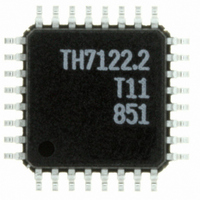
TH7122ENE Melexis Inc, TH7122ENE Datasheet - Page 17

TH7122ENE
Manufacturer Part Number
TH7122ENE
Description
IC TXRX 930MHZ FSK/FM/ASK 32LQFP
Manufacturer
Melexis Inc
Specifications of TH7122ENE
Frequency
300MHz ~ 930MHz
Data Rate - Maximum
115Kbps
Modulation Or Protocol
ASK, FM, FSK
Applications
Alarm and Security Systems, RKE, TPMS
Power - Output
-10dBm ~ 11dBm
Sensitivity
-105dBm
Voltage - Supply
2.2 V ~ 5.5 V
Current - Receiving
14mA
Current - Transmitting
23mA @ 10dBm
Data Interface
PCB, Surface Mount
Antenna Connector
PCB, Surface Mount
Operating Temperature
-40°C ~ 85°C
Package / Case
32-LQFP
Transmitting Current
12mA
Data Rate
115Kbps
Frequency Range
300MHz To 930MHz
Modulation Type
AM, FM, FSK
Sensitivity Dbm
-105dBm
Rf Ic Case Style
LQFP
No. Of Pins
32
Supply Voltage
RoHS Compliant
Output Power
10dBm
Rohs Compliant
Yes
Lead Free Status / RoHS Status
Lead free / RoHS Compliant
Memory Size
-
Lead Free Status / RoHS Status
Lead free / RoHS Compliant
Other names
TH7122.3
TH7122ENETR
TH7122ENETR
Available stocks
Company
Part Number
Manufacturer
Quantity
Price
3.3.5
FSK modulation can be achieved by pulling the crystal oscillator
frequency. A CMOS-compatible data stream applied at pin
IN_DTA digitally modulates the XOSC via an integrated NMOS
switch. Two external pulling capacitors CX1 and CX2 allow the
FSK deviation Δf and center frequency f
pendently. At IN_DTA = LOW CX2 is connected in parallel to CX1
leading to the low-frequency component of the FSK spectrum
(f
is set to its high frequency, leading to f
An external reference signal can be directly AC-coupled to the reference oscillator input pin RO. Then the
transceiver is used without a XTAL. Now the reference signal sets the carrier frequency and has to contain
the FSK (or FM) modulation
Alternatively FSK or FM can be achieved by injecting the modu-
lating signal into the loop filter to directly control the VCO fre-
quency. Fig. 10 shows a circuit proposal for direct VCO modula-
tion. This circuit is recommended for data rates in excess of about
20 kbps NRZ. An external VCO tuning varactor should be added
for narrow-band applications, for example at channel spacings of
25 kHz. For details please refer to the application notes “TH7122
and TH71221 High Speed Data Communication” and “TH7122
and TH71221 Used In Narrow Band FSK Applications” as well as
to the “TH7122 and TH71221 Cookbook”
Fig. 10: Circuit schematic for direct VCO modulation
3.3.6
A crystal is tuned by the manufacturer to the re-
quested oscillation frequency f
capacitance CL within the specified calibration
tolerance. The only way to tune this oscillation
frequency is to vary the effective load capacitance
CL
Figure 8 shows the oscillation frequency of a crys-
tal in dependency on the effective load capaci-
tance. This capacitance changes in accordance
with the logic level of IN_DTA around the specified
load capacitance. The figure illustrates the rela-
tionship between the external pulling capacitors
and the frequency deviation.
39010 07122
Rev. 010
min
IN_DTA
eff
); while at IN_DTA = HIGH CX2 is deactivated and the XOSC
seen by the crystal.
0
1
FSK Modulation
•
•
Crystal Tuning
Fig. 11: Crystal Tuning Characteristic
FSK modulation via crystal pulling
FSK modulation via direct VCO modulation
f
f
min
max
= f
= f
c
c
- Δf (FSK switch is closed)
+ Δf (FSK switch is open)
0
Description
for a certain load
max
.
c
to be adjusted inde-
Page 17 of 44
f
f
max
min
f
o
f
CX1 CRO
CX1+CRO
FSK/FM/ASK Transceiver
VCC
CM1
CL
Fig. 9:
IN_DTA
RF
CF2
CX2
CX1
XTAL
(CX1+CX2) CRO
CX1+CX2+CRO
FSKSW
RM1
RO
Crystal Pulling Circuit
CB6
C1
L0
L1
XTAL
CF1
R1
27 to 930MHz
36pF
TH7122
VCC
VEE
17
18
20
22
23
24
19
21
C0
VEE_DIG
FS1/LD
Data Sheet
FS0/SDEN
VCC_PLL
TNK_LO
VEE_PLL
LF
I
RO
36pF
Feb/09
CL
CL
eff
eff


