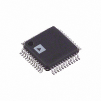
AD9874ABST Analog Devices Inc, AD9874ABST Datasheet - Page 38

AD9874ABST
Manufacturer Part Number
AD9874ABST
Description
IC IF DIGIT SUBSYSTEM 48-LQFP
Manufacturer
Analog Devices Inc
Datasheet
1.AD9874-EB.pdf
(40 pages)
Specifications of AD9874ABST
Frequency
10MHz ~ 300MHz
Rohs Status
RoHS non-compliant
Function
IF Digitizing Subsystem
Rf Type
UHF, Cellular, TETRA, GSM, EDGE, APCO25
Secondary Attributes
16dB Front End Attenuator
Package / Case
48-LQFP
Ic Function
A/D Converter (A-D)
Supply Voltage Range
2.7V To 3.6V
Operating Temperature Range
-40°C To +85°C
Digital Ic Case Style
LQFP
No. Of Pins
48
Msl
MSL 3 - 168 Hours
For Use With
AD9874-EB - BOARD EVAL FOR AD9874
Lead Free Status / RoHS Status
Lead free / RoHS Compliant
Available stocks
Company
Part Number
Manufacturer
Quantity
Price
Company:
Part Number:
AD9874ABST
Manufacturer:
AD
Quantity:
672
Part Number:
AD9874ABST
Manufacturer:
ADI/亚德诺
Quantity:
20 000
Part Number:
AD9874ABSTZ
Manufacturer:
ADI/亚德诺
Quantity:
20 000
AD9874
results in a
point difference to be calibrated to exactly 24 dB, so that a
simple 5-bit shift would make up the gain difference. The
attenuated path can handle signal levels up to –12 dB at the
antenna before being overdriven. Since the SAW filters provide
sufficient blocker suppression, the digital data from this path
need only be selected when the target signal exceeds –36 dBm.
Although the sensitivity of the receiver with the attenuated path
is 20 dB lower than the direct path, the strong target signal
ensures a sufficiently high carrier-to-noise ratio.
Since GSM is based on a TDMA scheme, digital data (or path)
selection can occur on a slot-by-slot basis. The AD9874 would
be configured to provide Serial I and Q data at a frame rate of
541.67 kSPS, as well as additional information including a 2-bit
reset field and a 6-bit RSSI field. These two fields contain the
information needed to decide whether the direct or attenuated
path should be used for the current time slot.
Hung Mixer Mode
The AD9874 can be operated in the hung mixer mode by tying
one of the LO’s self-biasing inputs to ground (i.e., GNDI) or
the positive supply (VDDI). In this mode, the AD9874 acts as a
narrow-band, band-pass - ADC, since its mixer passes the
IFIN signal without any frequency translation. The IFIN signal
must be centered about the resonant frequency of the - ADC
(i.e., f
must be selected to accommodate the bandwidth of the desired
input signal. Note that the LO synthesizer can be disabled
because it is no longer required.
Since the mixer does not have any losses associated with the
mixing operation, the conversion gain through the LNA and
mixer is higher resulting in a nominal input clip point of
–24 dBm. The linearity or IIP3 performance of the LNA and
mixer remains roughly unchanged and similar to that shown
in Figure 11b. The SNR performance is dependent of the
VGA attenuation setting, I/Q data resolution, and output
bandwidth as shown in Figure 30. Applications requiring the
highest instantaneous dynamic range should set the VGA for
maximum attenuation. Also, several extra decibels in SNR
performance can be gained at lower signal bandwidths by
using 24-bit I/Q data.
CLK
Figure 30. Hung Mixer SNR vs. BW and VGA
105
100
95
90
85
80
/8) and the clock rate, f
0
6 dB adjustment of the clip point, allowing the clip
20
16-BIT I/Q DATA
MAX ATTEN w/
24-BIT I/Q DATA
MIN ATTEN w/
40
60
24-BIT I/Q DATA
BW – kHz
MAX ATTEN w/
CLK
80
, and decimation factors
100
16-BIT I/Q DATA
f
MIN ATTEN w/
120
CLK
= 18MSPS
140
160
–38–
LAYOUT EXAMPLE, EVALUATION BOARD, AND
SOFTWARE
The evaluation board and its accompanying software provide
a simple way to evaluate the AD9874. The block diagram in
Figure 31 shows the major blocks of the evaluation board,
which is designed to be flexible, allowing configuration for
different applications.
The power supply distribution block provides filtered, adjustable
voltages to the various supply pins of the AD9874. In the IF
input signal path, component pads are available to implement
different IF impedance matching networks. The LO and CLK
signals can be externally applied or internally derived from a
user-supplied VCO module interface daughter board. The refer-
ence for the on-chip LO and CLK synthesizers can be applied
via the external f
The evaluation board is designed to interface to a PC via a
National Instruments NI 6533 digital IO card. An XILINX
FPGA formats the data between the AD9874 and digital
I/O card.
Software developed using National Instruments’ LabVIEW™
(and provided as Microsoft
is supplied for the configuration of the SPI port registers and
evaluation of the AD9874 output data. These programs have
a convenient graphical user interface that allows for easy access
to the various SPI port configuration registers and real-time
frequency analysis of the output data.
For more information on the AD9874 evaluation board, includ-
ing an example layout, please refer to the EVAL-AD9874EB
Data Sheet.
OUTPUT
POWER SUPPLY
MIXER
DISTRIBUTION
Figure 31. Evaluation Board Platform
INPUT
IF
REF
DUT
input or an on-board crystal oscillator.
INPUT
INPUT
LO
CLK
®
AD9874
EPROM
Windows
SPARTON
XILINX
FPGA
INTERFACE
®
MODULE
OSCILLATOR
(OPTIONAL)
executable programs)
(OPTIONAL)
VCO
CRYSTAL
FIFO
IDT
INPUT
FREF
REV. A


