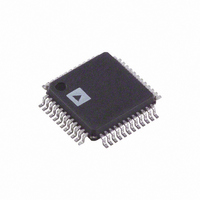
AD9874ABST Analog Devices Inc, AD9874ABST Datasheet - Page 26

AD9874ABST
Manufacturer Part Number
AD9874ABST
Description
IC IF DIGIT SUBSYSTEM 48-LQFP
Manufacturer
Analog Devices Inc
Datasheet
1.AD9874-EB.pdf
(40 pages)
Specifications of AD9874ABST
Frequency
10MHz ~ 300MHz
Rohs Status
RoHS non-compliant
Function
IF Digitizing Subsystem
Rf Type
UHF, Cellular, TETRA, GSM, EDGE, APCO25
Secondary Attributes
16dB Front End Attenuator
Package / Case
48-LQFP
Ic Function
A/D Converter (A-D)
Supply Voltage Range
2.7V To 3.6V
Operating Temperature Range
-40°C To +85°C
Digital Ic Case Style
LQFP
No. Of Pins
48
Msl
MSL 3 - 168 Hours
For Use With
AD9874-EB - BOARD EVAL FOR AD9874
Lead Free Status / RoHS Status
Lead free / RoHS Compliant
Available stocks
Company
Part Number
Manufacturer
Quantity
Price
Company:
Part Number:
AD9874ABST
Manufacturer:
AD
Quantity:
672
Part Number:
AD9874ABST
Manufacturer:
ADI/亚德诺
Quantity:
20 000
Part Number:
AD9874ABSTZ
Manufacturer:
ADI/亚德诺
Quantity:
20 000
AD9874
Once the AD9874 has been tuned, the noise figure degradation
attributed solely to the temperature drift of the LC and RC
resonators is minimal. Since the drift of the RC resonator is
actually negligible compared to that of the LC resonator, the
external L and C components’ temperature drift characteristics
tend to dominate. Figure 13d shows the degradation in noise
figure as the product of the LC value is allowed to vary from
–12.5% to +12.5%. Note that the noise figure remains relatively
constant over a
that most applications will not be required to retune over the
operating temperature range.
DECIMATION FILTER
The decimation filter shown in Figure 14 consists of an f
complex mixer and a cascade of three linear phase FIR filters:
DEC1, DEC2, and DEC3. DEC1 downsamples by a factor of
12 using a fourth order comb filter. DEC2 also uses a fourth
order comb filter, but its decimation factor is set by the M field
of Register 0x07. DEC3 is either a decimate-by-5 FIR filter or a
decimate-by-4 FIR filter, depending on the value of the K bit
within Register 0x07. Thus, the composite decimation factor
can be set to either 60
respectively.
The output data rate (f
frequency (f
Due to the transition region associated with the decimation
filter’s frequency response, the decimation factor must be
selected such that f
signal bandwidth. This ensures low amplitude ripple in the pass
band along with the ability to provide further application-spe-
cific digital filtering prior to demodulation.
MODULATOR
FROM -
Figure 13d. Typical Noise Figure Degradation
from L and C Component Drift (f
f
DATA
IF
12
11
10
= 73.3501 MHz)
9
8
Figure 14. Decimation Filter Architecture
–15
CLK
COS
SIN
) divided by the digital filter’s decimation factor.
BW = 10kHz
–10
3.5% range (i.e., 35,000 ppm), suggesting
OUT
SINC
FILTER
BW = 75kHz
DEC1
4
OUT
is equal to or greater than twice the
M or 48
–5
12
) is equal to the modulator clock
LC ERROR – %
SINC
FILTER
BW = 30kHz
0
DEC2
4
M for K equal to 0 or 1,
M
M + 1
5
CLK
= 18 MSPS,
FIR
FILTER
DEC3
10
K
OR
4
5
COMPLEX
DATA TO
SSI PORT
Q
I
15
CLK
/8
–26–
Figure 15a shows the response of the decimation filter at a
decimation factor of 900 (K = 0, M = 14) and a sampling
clock frequency of 18 MHz. In this example, the output data
rate (f
width of 10 kHz centered around dc. As this figure shows,
the first and second alias bands (occurring at even integer
multiples of f
least 88 dB of attenuation. Note that signals falling around
frequency offsets that are odd integer multiples of f
(i.e., 10 kHz, 30 kHz, and 50 kHz) will fall back into the
transition band of the digital filter.
Figure 15b shows the response of the decimation filter with a
decimation factor of 48 and a sampling clock rate of 26 MHz. The
alias attenuation is at least 94 dB and occurs for frequencies at the
edges of the fourth alias band. The difference between the alias
attenuation characteristics of Figure 15b and those of Figure 15a is
due to the fact that the third decimation stage decimates by a factor
of 5 for Figure 15a compared with a factor of 4 for Figure 15b.
Figure 15a. Decimation Filter Frequency Response
for f
Figure 15b. Decimation Filter Frequency Response
for f
OUT
–100
–120
–100
–120
–20
–40
–60
–80
–20
–40
–60
–80
0
) is 20 kSPS, with a usable complex signal band-
0
OUT
OUT
0
0
FOLD-
POINT
ING
OUT
= 20 kSPS (f
= 541.666 kSPS (f
10
/2) have the least attenuation but provide at
–98dB
20
0.5
5.0kHz PASS BAND
–88dB
135.466kHz PASS BAND
30
FREQUENCY – kHz
CLK
FREQUENCY – MHz
1.0
–115dB
40
–88dB
= 18 MHz, OSR = 900)
CLK
50
= 26 MHz, OSR = 48)
1.5
60
–101dB
70
2.0
–94dB
80
–103dB
90
OUT
2.5
REV. A
100
/2


