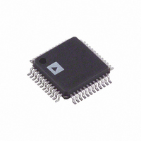
AD9874ABST Analog Devices Inc, AD9874ABST Datasheet - Page 15

AD9874ABST
Manufacturer Part Number
AD9874ABST
Description
IC IF DIGIT SUBSYSTEM 48-LQFP
Manufacturer
Analog Devices Inc
Datasheet
1.AD9874-EB.pdf
(40 pages)
Specifications of AD9874ABST
Frequency
10MHz ~ 300MHz
Rohs Status
RoHS non-compliant
Function
IF Digitizing Subsystem
Rf Type
UHF, Cellular, TETRA, GSM, EDGE, APCO25
Secondary Attributes
16dB Front End Attenuator
Package / Case
48-LQFP
Ic Function
A/D Converter (A-D)
Supply Voltage Range
2.7V To 3.6V
Operating Temperature Range
-40°C To +85°C
Digital Ic Case Style
LQFP
No. Of Pins
48
Msl
MSL 3 - 168 Hours
For Use With
AD9874-EB - BOARD EVAL FOR AD9874
Lead Free Status / RoHS Status
Lead free / RoHS Compliant
Available stocks
Company
Part Number
Manufacturer
Quantity
Price
Company:
Part Number:
AD9874ABST
Manufacturer:
AD
Quantity:
672
Part Number:
AD9874ABST
Manufacturer:
ADI/亚德诺
Quantity:
20 000
Part Number:
AD9874ABSTZ
Manufacturer:
ADI/亚德诺
Quantity:
20 000
SERIAL PORT INTERFACE (SPI)
The serial port of the AD9874 has 3-wire or 4-wire SPI capability,
allowing read/write access to all registers that configure the
device’s internal parameters. The default 3-wire serial commu-
nication port consists of a clock (PC), peripheral enable (PE), and
bidirectional data (PD) signal. The inputs to PC, PE, and PD
contain a Schmitt trigger with a nominal hysteresis of 0.4 V
centered about the digital interface supply (i.e., VDDH/2).
A 4-wire SPI interface can be enabled by setting the MSB of the
SSICRB register (Reg. 0x19, Bit 7), resulting in the output data
also appearing on the DOUTB pin. Note that since the default
power-up state sets DOUTB low, bus contention is possible for
systems sharing the SPI output line. To avoid any bus contention,
the DOUTB pin can be three-stated by setting the fourth control
bit in the three-state bit (Reg 0x3B, Bit 3). This bit can then be
toggled to gain access to the shared SPI output line.
An 8-bit instruction header must accompany each read and
write SPI operation. Only the write operation supports an auto-
increment mode, allowing the entire chip to be configured in a
single write operation. The instruction header is shown in
Table II. It includes a read/not-write indicator bit, six address
bits, and a don’t care bit. The data bits immediately follow the
instruction header for both read and write operations. Note that
the address and data are always given MSB first.
MSB
I7
R/W
Figure 1a illustrates the timing requirements for a write opera-
tion to the SPI port. After the peripheral enable (PE) signal goes
low, data (PD) pertaining to the instruction header is read on
the rising edges of the clock (PC). To initiate a write operation,
the read/not-write bit is set low. After the instruction header is
read, the eight data bits pertaining to the specified register are
REV. A
I6
A5
Table II. Instruction Header Information
DOUTB
PC
PD
PE
I5
A4
PC
PD
PE
I4
A3
DON’T
CARE
I3
A2
t
DS
t
DS
t
S
t
I2
A1
S
R/W
t
DON’T
HI
CARE
R/W
t
t
t
DH
Figure 1a. SPI Write Operation Timing
CLK
Figure 1b. SPI Read Operation Timing
HI
t
DH
t
t
CLK
LOW
t
I1
A0
LOW
DON’T
CARE
A5
A5
LSB
I0
X
A1
A4
DON’T
CARE
–15–
A0
A0
shifted into the data pin (PD) on the rising edge of the next
eight clock cycles. PE stays low during the operation and goes
high at the end of the transfer. If PE rises before the eight clock
cycles have passed, the operation is aborted.
If PE stays low for an additional eight clock cycles, the destina-
tion address is incremented and another eight bits of data are
shifted in. Again, should PE rise early, the current byte is
ignored. By using this implicit addressing mode, the entire
chip can be configured with a single write operation. Regis-
ters identified as being subject to frequent updates, namely
those associated with power control and AGC operation, have
been assigned adjacent addresses to minimize the time required
to update them. Note that multibyte registers are big-endian
(the most significant byte has the lower address) and are updated
when a write to the least significant byte occurs.
Figure 1b illustrates the timing for a read operation to the SPI
port. Although the AD9874 does not require read access for
proper operation, it is often useful in the product development
phase or for system authentication. Note that the readback
enable bit (Register 0x3A, Bit 3) must be set for a read opera-
tion with a 3-wire SPI interface. After the peripheral enable
(PE) signal goes low, data (PD) pertaining to the instruction
header is read on the rising edges of the clock (PC). A read
operation occurs if the read/not-write indicator is set high. After
the address bits of the instruction header are read, the eight data
bits pertaining to the specified register are shifted out of the
data pin (PD) on the falling edges of the next eight clock cycles.
If the 4-wire SPI interface is enabled, the eight data bits will
also appear on the DOUTB pin with the same timing relation-
ship as those appearing at PD. After the last data bit is shifted
out, the user should return PE high, causing PD to become
three-stated and return to its normal status as an input pin.
Since the auto increment mode is not supported for read opera-
tions, an instruction header is required for each register read
operation and PE must return high before initiating the next
read operation.
DON’T
CARE
DON’T
DON’T
CARE
CARE
t
DV
D7
D7
D7
D6
D6
D6
D1
D1
D1
t
H
D0
D0
D0
t
EZ
DON’T
CARE
AD9874


