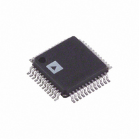
AD9874ABST Analog Devices Inc, AD9874ABST Datasheet - Page 17

AD9874ABST
Manufacturer Part Number
AD9874ABST
Description
IC IF DIGIT SUBSYSTEM 48-LQFP
Manufacturer
Analog Devices Inc
Datasheet
1.AD9874-EB.pdf
(40 pages)
Specifications of AD9874ABST
Frequency
10MHz ~ 300MHz
Rohs Status
RoHS non-compliant
Function
IF Digitizing Subsystem
Rf Type
UHF, Cellular, TETRA, GSM, EDGE, APCO25
Secondary Attributes
16dB Front End Attenuator
Package / Case
48-LQFP
Ic Function
A/D Converter (A-D)
Supply Voltage Range
2.7V To 3.6V
Operating Temperature Range
-40°C To +85°C
Digital Ic Case Style
LQFP
No. Of Pins
48
Msl
MSL 3 - 168 Hours
For Use With
AD9874-EB - BOARD EVAL FOR AD9874
Lead Free Status / RoHS Status
Lead free / RoHS Compliant
Available stocks
Company
Part Number
Manufacturer
Quantity
Price
Company:
Part Number:
AD9874ABST
Manufacturer:
AD
Quantity:
672
Part Number:
AD9874ABST
Manufacturer:
ADI/亚德诺
Quantity:
20 000
Part Number:
AD9874ABSTZ
Manufacturer:
ADI/亚德诺
Quantity:
20 000
DW
0 (16-bit) 0
1 (24-bit) 0
*The number of bits per frame with embedded frame sync (EFS = 1) assume at
The maximum SSIORD setting can be determined by the equation
where TRUNC is the truncated integer value.
Table IV lists the number of bits within a frame for 16-bit and
24-bit output data formats for all of the different SSICR set-
tings. The decimation factor is determined by the contents of
Register 0x07.
REV. A
least 10 idle bits are desired.
Number of Bits per Frame for Different SSICR Settings
(#
SSIORD TRUNC Dec Factor
of Bits per Frame
EAGC
0
1
1
1
1
0
1
1
1
1
≤
IDLE (HIGH) BITS
CLKOUT
CLKOUT
CLKOUT
CLKOUT
DOUT
DOUT
DOUT
DOUT
FS
FS
FS
FS
EFS
0
1
0
0
1
1
0
1
0
0
1
1
)}
{(
Figure 3a. SSI Timing for Several SSICRA Settings with 16-Bit I/Q Data
Table IV.
SCKI = 0, SCKT = 0, SLFS = 0, SFSI = 0, EFS = 0, SFST = 0, EAGC = 0
SCKI = 0, SCKT = 0, SLFS = 0, SFSI = 0, EFS = 0, SFST = 0, EAGC = 1, AAGC = 0
SCKI = 0, SCKT = 0, SLFS = X, SFSI = X, EFS = 1, SFST = 1, EAGC = 0
SCKI = 0, SCKT = 0, SLFS = X, SFSI = X, EFS = 1, SFST = 0, EAGC = 0: AS ABOVE, BUT FS IS LOW
SCKI = 0, SCKT = 0, SLFS = 1, SFSI = 0, EFS = 0, SFST = 0, EAGC = 0
.
START
AAGC
NA
NA
0
1
0
1
NA
NA
0
1
0
1
BIT
) /
I15
I15
I15
I15
Number of Bits
per Frame
32
49*
48
40
69*
59*
48
69*
64
56
89*
79*
I0
I0
I0
I8
HI-Z
Q15
STOP
Q15
BIT
Q15
(1)
–17–
START
Q14
Q14
BIT
Q14
An example helps illustrate how the maximum SSIORD setting
is determined. Suppose a user selects a decimation factor of 600
(Register 0x07, K = 0, M = 9) and prefers a 3-wire interface
with a dedicated frame sync (EFS = 0) containing 24-bit data
(DW = 1) with nonalternating embedded AGC data included
(EAGC = 1, AAGC = 0). Referring to Table IV, each frame
will consist of 64 data bits. Using Equation 1, the maximum
SSIORD setting is 9 (= TRUNC(600/64)). Thus, the user
can select any SSIORD setting between 1 and 9.
Figure 3a illustrates the output timing of the SSI port for several
SSI control register settings with 16-bit I/Q data, while Figure 3b
shows the associated timing parameters. Note that the same timing
relationship holds for 24-bit I/Q data, with the exception that I
and Q word lengths now become 24 bits. In the default mode of
the operation, data is shifted out on rising edges of CLKOUT
after a pulse equal to a clock period is output from the Frame
Sync (FS) pin. As described above, the output data consists of a
16- or 24-bit I sample followed by a 16- or 24-bit Q sample,
plus two optional bytes containing AGC and status information.
*Timing parameters also apply to inverted CLKOUT or FS modes, with t
relative to the falling edge of the CLK and/or FS.
Q0
Q0
I7
Q0
Figure 3b. Timing Parameters for SSI Timing*
CLKOUT
DOUT
ATTN7
FS
I0
ATTEN6
t
STOP
t
V
BIT
HI
t
CLK
t
DV
t
LOW
START
RSSI0
BIT
I15
Q15
I14
AD9874
DV


