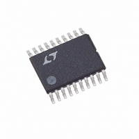
LT5514EFE Linear Technology, LT5514EFE Datasheet - Page 9

LT5514EFE
Manufacturer Part Number
LT5514EFE
Description
IC IF AMP/ADC DRVR PROG 20TSSOP
Manufacturer
Linear Technology
Datasheet
1.LT5514EFE.pdf
(20 pages)
Specifications of LT5514EFE
Function
Amplifier/ADC Driver
Frequency
LF ~ 850MHz
Secondary Attributes
Max Output 21dBm
Package / Case
20-TSSOP (0.173", 4.40mm Width) Exposed Pad
Lead Free Status / RoHS Status
Contains lead / RoHS non-compliant
Available stocks
Company
Part Number
Manufacturer
Quantity
Price
Part Number:
LT5514EFE
Manufacturer:
LINEAR/凌特
Quantity:
20 000
Company:
Part Number:
LT5514EFE#PBF
Manufacturer:
MAX
Quantity:
60
Part Number:
LT5514EFE#PBF
Manufacturer:
LINEAR/凌特
Quantity:
20 000
Part Number:
LT5514EFE#TRPBF
Manufacturer:
LINEAR/凌特
Quantity:
20 000
ENA = ENB = 3V, control input levels V
noted. Note 1: Subtract 0.75ns calibration delay from output plots to estimate the LT5514 group delay. Note 2: When specified, C
is connected differentially across the LT5514 OUT
TYPICAL PERFOR A CE CHARACTERISTICS
Pulse Response vs C
Gain. Output Level is 2V
50 External Load
R
INPUT
MATCH
0pF
= 255
GROUND
22pF TO
OUTPUT
EACH
2ns/DIV
Pulse Response vs Attenuation,
Output Level is 2V
into 50 External Load
Pulse Response vs Attenuation,
LT5514 Levels are: V
V
R
FIGURE 9 TEST CIRCUIT
R
OUT
OUT
INPUT
INPUT
MATCH
OUT
= 100
= 2V
P-P
at Max
= 255
W
P-P
into
C
0pF
1pF
1.8pF
3.3pF
4.7pF
6.8pf
10pF
11pF
18pF
OUT
5514 G27
at Max Gain
1ns/DIV
1ns/DIV
U
IL
= 0.6V, V
P-P
IN
at Max Gain
= 66mV
MAX GAIN
1.5dB STEP
3dB STEP
6dB STEP
12dB STEP
MAX GAIN
1.5dB STEP
3dB STEP
6dB STEP
12dB STEP
IH
+
, OUT
= 3V unless otherwise noted. Test circuit shown in Figure 10 unless otherwise
Pulse Response vs Output Level at
Max Gain. Indicated Voltage
Levels are into 50 External Load
C
INPUTS
5514 G32
5514 G30
OUT
P-P
–
= 0.82pF
,
output pins.
2ns/DIV
4V
3V
2V
P-P
P-P
P-P
Pulse Response vs Attenuation,
Output Level is 2V
into 50 External Load
Pulse Response vs Attenuation,
LT5514 Levels are: V
V
R
R
FIGURE 9 TEST CIRCUIT
OUT
(Standard Mode) T
INPUT
MATCH
OUT
INPUT
5514 G28
= 200
= 4V
= 255 , C
P-P
at Max Gain
OUT
1ns/DIV
1ns/DIV
= 1.8pF
P-P
Pulse Response vs Attenuation,
Output Level is 4V
into 50 External Load
INPUT
A
at Max Gain
IN
= 25 C, V
= 66mV
MAX GAIN
1.5dB STEP
3dB STEP
6dB STEP
12dB STEP
MAX GAIN
1.5dB STEP
3dB STEP
6dB STEP
12dB STEP
5514 G31
5514 G33
P-P
CC
1ns/DIV
,
= 5V, V
P-P
at Max Gain
LT5514
CCO
MAX GAIN
1.5dB STEP
3dB STEP
6dB STEP
12dB STEP
= 5V,
5514 G29
OUT
9
5514f


