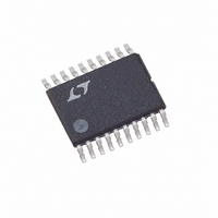
LT5514EFE Linear Technology, LT5514EFE Datasheet - Page 19

LT5514EFE
Manufacturer Part Number
LT5514EFE
Description
IC IF AMP/ADC DRVR PROG 20TSSOP
Manufacturer
Linear Technology
Datasheet
1.LT5514EFE.pdf
(20 pages)
Specifications of LT5514EFE
Function
Amplifier/ADC Driver
Frequency
LF ~ 850MHz
Secondary Attributes
Max Output 21dBm
Package / Case
20-TSSOP (0.173", 4.40mm Width) Exposed Pad
Lead Free Status / RoHS Status
Contains lead / RoHS non-compliant
Available stocks
Company
Part Number
Manufacturer
Quantity
Price
Part Number:
LT5514EFE
Manufacturer:
LINEAR/凌特
Quantity:
20 000
Company:
Part Number:
LT5514EFE#PBF
Manufacturer:
MAX
Quantity:
60
Part Number:
LT5514EFE#PBF
Manufacturer:
LINEAR/凌特
Quantity:
20 000
Part Number:
LT5514EFE#TRPBF
Manufacturer:
LINEAR/凌特
Quantity:
20 000
PACKAGE DESCRIPTIO
APPLICATIO S I FOR ATIO
At high frequency, the difference between the top and
bottom curves in Figure 12 is simply power loss. Starting
from the LT5514 intrinsic performance at R
(top curve), the next lower curve takes into account the
transformer insertion loss. The next curve below this
shows the LT5514 OIP3 with R
curve in the plot includes the effects of transformer
insertion loss, with R
of loss due to R
The transformer board can provide a differential output
when Jumper J2 is removed.
MATCH
6.60 0.10
(.0035 – .0079)
U
0.09 – 0.20
NOTE:
1. CONTROLLING DIMENSION: MILLIMETERS
2. DIMENSIONS ARE IN
3. DRAWING NOT TO SCALE
OUT
4.50 0.10
.
= 100 , and the additional effect
RECOMMENDED SOLDER PAD LAYOUT
U
Information furnished by Linear Technology Corporation is believed to be accurate and reliable.
However, no responsibility is assumed for its use. Linear Technology Corporation makes no represen-
tation that the interconnection of its circuits as described herein will not infringe on existing patent rights.
(.169 – .177)
4.30 – 4.50*
OUT
(.020 – .030)
0.50 – 0.75
SEE NOTE 4
W
(.152)
= 100 . The bottom
MILLIMETERS
3.86
U
(INCHES)
0.65 BSC
20-Lead Plastic TSSOP (4.4mm)
(Reference LTC DWG # 05-08-1663)
0.45 0.05
OUT
U
Exposed Pad Variation CB
(.108)
0.25
REF
2.74
= 200
1.05 0.10
0 – 8
*DIMENSIONS DO NOT INCLUDE MOLD FLASH. MOLD FLASH
4. RECOMMENDED MINIMUM PCB METAL SIZE
SHALL NOT EXCEED 0.150mm (.006") PER SIDE
FE Package
FOR EXPOSED PAD ATTACHMENT
The Wideband Differential Output Application Board (Fig-
ure 11) is an example of direct coupling (no transformer)
to the load, and has wider output bandwidth. This board
gives direct access to the LT5514’s output pins, and was
used for stability tests. Higher V
compensate for the DC voltage drop on R1 and R2. Use
TP2, TP3 to monitor the actual LT5514 output bias volt-
age. By replacing R1 and R2 with inductors, this board can
operate with a 5V supply. However, this may limit the
minimum signal frequency. For example, an 820nH choke
inductor will limit the lowest signal frequency to 40MHz.
(.0256)
0.65
BSC
20 1918 17 16 15
1
(.0077 – .0118)
0.195 – 0.30
2
TYP
3 4 5 6 7 8 9 10
(.252 – .260)
6.40 – 6.60*
(.152)
3.86
14 13
12
11
FE20 (CB) TSSOP 0204
(.002 – .006)
0.05 – 0.15
(.108)
(.047)
2.74
MAX
1.20
OSUP
(.252)
6.40
BSC
(7V) is required to
LT5514
19
5514f


