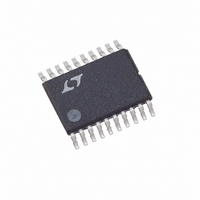
LT5514EFE Linear Technology, LT5514EFE Datasheet

LT5514EFE
Specifications of LT5514EFE
Available stocks
Related parts for LT5514EFE
LT5514EFE Summary of contents
Page 1
... AC response when driving capacitive loads, and excellent reverse isolation. The LT5514 may be operated broadband, where the out- put differential RC time constant sets the bandwidth may be used as a narrowband driver with the appropriate output filter. , LTC and LT are registered trademarks of Linear Technology Corporation. 5V CHOKE CHOKE 0.1 F 100 ...
Page 2
... Low High Low High Low Low High Low Low Low Low Low Low Low Low U W INFORMATION ORDER PART TOP VIEW NUMBER 1 20 ENB CC2 LT5514EFE 3 18 GND 4 17 GND + – OUT 21 – OUT 7 14 GND 8 13 GND 9 12 PGA3 10 11 ...
Page 3
DC ELECTRICAL CHARACTERISTICS noted. (Note 7) (Test circuits shown in Figures 9 and 10) SYMBOL PARAMETER Normal Operating Conditions V Supply Voltage (Pins 2, 19 – V OUT , OUT Output Pin DC Common Mode Voltage CCO + ...
Page 4
LT5514 AC ELECTRICAL CHARACTERISTICS 5V, ENA = ENB = 3V CCO and differential outputs, unless otherwise noted. (Note 7) (Test circuits shown in Figures 9 and 10) SYMBOL PARAMETER Dynamic Performance BW Large-Signal ...
Page 5
AC ELECTRICAL CHARACTERISTICS 5V, ENA = 3V, ENB = 0.6V CCO inputs and differential outputs, unless otherwise noted. (Note 7) (Test circuits shown in Figures 9 and 10) SYMBOL PARAMETER Dynamic Performance BW ...
Page 6
LT5514 W U TYPICAL PERFOR A CE CHARACTERISTICS ENA = ENB = 3V, control input levels V IL Frequency Response for All Gain Steps 100 OUT ...
Page 7
W U TYPICAL PERFOR A CE CHARACTERISTICS ENA = ENB = 3V, control input levels V IL Minimum Gain 120MHz 100 OUT 7.8 7.6 7.4 – 6.8 ...
Page 8
LT5514 W U TYPICAL PERFOR A CE CHARACTERISTICS ENA = ENB = 5V 5V CCO in Figure 10) OIP3 vs Frequency –23dBm IN Max Gain 200 ...
Page 9
W U TYPICAL PERFOR A CE CHARACTERISTICS ENA = ENB = 3V, control input levels V IL noted. Note 1: Subtract 0.75ns calibration delay from output plots to estimate the LT5514 group delay. Note 2: When specified connected ...
Page 10
LT5514 W U TYPICAL PERFOR A CE CHARACTERISTICS ENA = 3V, ENB = 0.6V or ENA = 0.6V, ENB = 3V, control input levels V Figure 10) OIP3 vs Frequency at Pin = –23dBm, Max Gain and 1.5dB Attenuation Step, ...
Page 11
CTIO S ENA (Pin 1): Enable Pin for Amplifier A. When the input voltage is higher than 3V, amplifier A is turned on. When the input voltage is less than or equal to 0.6V, amplifier ...
Page 12
LT5514 U U APPLICATIO S I FOR ATIO Circuit Operation The LT5514 is a high linearity amplifier with high imped- ance output (Figure 1). It consists of the following sections: • An input variable attenuator “gain-control” block with 100 input ...
Page 13
U U APPLICATIO S I FOR ATIO Input Interface For the lowest noise and highest linearity, the LT5514 should be driven with a differential input signal. Single- ended drive will severely degrade linearity and noise performance. Example input matching networks ...
Page 14
LT5514 U U APPLICATIO S I FOR ATIO Clipping Free Operation The LT5514 is a class A amplifier. To avoid signal distor- tion, the user must ensure that the LT5514 outputs do not enter into current or voltage limiting. The ...
Page 15
U U APPLICATIO S I FOR ATIO gain output amplifier. The overall gain of the LT5514 is digitally controlled by means of four gain control pins with internal pull-down. Minimum gain is programmed when the gain control pins are set ...
Page 16
LT5514 U U APPLICATIO S I FOR ATIO For example, for R = 200 , L1 33nH results in OUT 500MHz bandwidth. The series inductor can extend the application bandwidth, but it provides no improvement in linearity performance. ...
Page 17
U U APPLICATIO S I FOR ATIO allowing all impedances to be scaled downward by a factor of two. The NF and power gain remain the same in this case, but the OIP3 increases by 3dB. Then, with a further ...
Page 18
LT5514 U U APPLICATIO S I FOR ATIO Rather, it represents a compromise that most accurately measures the actual operation of the part by itself, undistorted by the artifacts of the impedance transformation network external bandwidth limiting factors. ...
Page 19
... DIMENSIONS ARE IN 3. DRAWING NOT TO SCALE Information furnished by Linear Technology Corporation is believed to be accurate and reliable. However, no responsibility is assumed for its use. Linear Technology Corporation makes no represen- tation that the interconnection of its circuits as described herein will not infringe on existing patent rights. W ...
Page 20
... Baseband Bandwidth, 40MHz to 500MHz IF, 1.8V to 5.25V Supply, –7dB to 56dB Linear Power Gain www.linear.com Offset Control, Shutdown, Adjustable Gain Offset Control, Shutdown, Adjustable Offset Offset Control, Adjustable Gain and Offset LT/TP 0504 1K • PRINTED IN THE USA LINEAR TECHNOLOGY CORPORATION 2004 5514f ...


