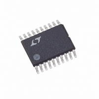
LT5514EFE Linear Technology, LT5514EFE Datasheet - Page 12

LT5514EFE
Manufacturer Part Number
LT5514EFE
Description
IC IF AMP/ADC DRVR PROG 20TSSOP
Manufacturer
Linear Technology
Datasheet
1.LT5514EFE.pdf
(20 pages)
Specifications of LT5514EFE
Function
Amplifier/ADC Driver
Frequency
LF ~ 850MHz
Secondary Attributes
Max Output 21dBm
Package / Case
20-TSSOP (0.173", 4.40mm Width) Exposed Pad
Lead Free Status / RoHS Status
Contains lead / RoHS non-compliant
Available stocks
Company
Part Number
Manufacturer
Quantity
Price
Part Number:
LT5514EFE
Manufacturer:
LINEAR/凌特
Quantity:
20 000
Company:
Part Number:
LT5514EFE#PBF
Manufacturer:
MAX
Quantity:
60
Part Number:
LT5514EFE#PBF
Manufacturer:
LINEAR/凌特
Quantity:
20 000
Part Number:
LT5514EFE#TRPBF
Manufacturer:
LINEAR/凌特
Quantity:
20 000
APPLICATIO S I FOR ATIO
Circuit Operation
The LT5514 is a high linearity amplifier with high imped-
ance output (Figure 1). It consists of the following
sections:
• An input variable attenuator “gain-control” block with
• Two parallel, differential transconductance amplifiers,
• An internal bias block with internal voltage regulator
• A gain control logic block
The LT5514 amplifier provides amplification with very low
distortion using a linearized open-loop architecture. In
contrast with high linearity amplifiers employing negative
feedback, the LT5514 offers:
• Stable operation for any practical load
• A capacitive output reactance (not inductive) that pro-
• Exceptional reverse isolation of –100dB at 50MHz and
The LT5514 is a transconductance amplifier and its opera-
tion can be understood conceptually as consisting of two
steps: First, the input signal voltage is converted to an
output current. The intermodulation distortion (in dBc) of
the LT5514 output current is determined by the input
signal level, and is almost independent of the output load
conditions. Thus, the LT5514’s input IP3 is also nearly
independent of the output load.
Next, the external output load (R
current to output voltage (or power). The LT5514’s volt-
age and power gain both increase with increasing R
Accordingly, the output power and output IP3 also im-
prove with increasing R
performance in the application will thus be set by the
choice of output load, as well as by the output network.
Maximum Gain Calculation
The maximum power gain (with the 0dB attenuation step)
is:
LT5514
12
100 input impedance
each with independent enable inputs
vides peaking free AC response to capacitive loads
–78dB at 300MHz (package and board leakage limited)
G
PWR
(dB) = 10 • log(g
U
OUT
m
U
2
. The actual output linearity
• R
IN
OUT
• R
W
) converts the output
OUT
)
U
OUT
.
where:
The power gain as a function of R
The ideal curves are straight lines. The curved lines
indicate the roll-off due to the finite (noninfinite) output
resistance of the LT5514.
The actual available output power (as well as power gain
and OIP3) will be reduced by losses in the output interface,
consisting of:
• The insertion loss of the output impedance transforma-
• About –3dB loss if a matching resistor (R
g
mode (0.15S in Low Power mode).
R
in Standard mode (122 in Low Power mode). Input
impedance matching is assumed.
R
seen by the LT5514’s differential outputs. R
be distinguished from the actual load impedance, R
which will typically be coupled to the LT5514 output by
an impedance transformation network.
tion network (for example the transformer insertion
loss in Figure 6)
Figure 6) is used to provide output load impedance
back-matching (for example when driving transmis-
sion lines)
m
IN
OUT
is the LT5514 transconductance = 0.3S in Standard
is the LT5514 differential input impedance 108
is the external differential output impedance as
Figure 2. Power Gain as a Function of R
45
40
35
30
25
20
15
10
5
0
20
100
R
OUT
( )
STANDARD MODE
LOW POWER MODE
STD WITH R
LP WITH R
OUT
is plotted in Figure 2.
O
1000 2000
O
5514 F02
OUT
OUT
MATCH
should
LOAD
5514f
in
,


