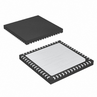
MAX16048ETN+ Maxim Integrated Products, MAX16048ETN+ Datasheet - Page 17

MAX16048ETN+
Manufacturer Part Number
MAX16048ETN+
Description
IC EE-PROG SYS MGR 8CH 56-TQFN
Manufacturer
Maxim Integrated Products
Type
System Managerr
Datasheet
1.MAX16046EVKIT.pdf
(70 pages)
Specifications of MAX16048ETN+
Number Of Voltages Monitored
8
Output
Open Drain, Push-Pull
Reset
Active Low
Reset Timeout
Adjustable/Selectable
Voltage - Threshold
Adjustable/Selectable
Operating Temperature
-40°C ~ 85°C
Mounting Type
Surface Mount
Package / Case
56-TQFN
Manual Reset
Resettable
Watchdog
Yes
Supply Voltage (max)
14 V
Supply Voltage (min)
3 V
Supply Current (typ)
6500 uA
Maximum Power Dissipation
3810 mW
Mounting Style
SMD/SMT
Maximum Operating Temperature
+ 85 C
Minimum Operating Temperature
- 40 C
Lead Free Status / RoHS Status
Lead free / RoHS Compliant
The MAX16046 is capable of managing up to twelve
system voltages simultaneously, and the MAX16048
can manage up to eight system voltages. After boot-
up, if EN is high and the Software Enable bit is set to
‘0,’ an internal multiplexer cycles through each input. At
each multiplexer stop, the 10-bit ADC converts the
monitored analog voltage to a digital result and stores
the result in a register. Each time the multiplexer finish-
es a conversion (8.3µs max), internal logic circuitry
compares the conversion results to the overvoltage and
undervoltage thresholds stored in memory. When a
conversion violates a programmed threshold, the con-
version can be configured to generate a fault. Logic
outputs can be programmed to depend on many com-
binations of faults. Additionally, faults are programma-
ble to trigger the nonvolatile fault logger, which writes
all fault information automatically to the EEPROM and
write-protects the data to prevent accidental erasure.
The MAX16046/MAX16048 contain both I
JTAG serial interfaces for accessing registers and
EEPROM. Use only one interface at any given time. For
more information on how to access the internal memory
through these interfaces, see the I
Serial Interface and JTAG Serial Interface sections.
Registers are divided into three pages with access con-
trolled by special I
The factory-default values at POR (power-on reset) for
all RAM registers are ‘0’s. POR occurs when V
es the undervoltage-lockout threshold (UVLO) of 2.85V
(max). At POR, the device begins a boot-up sequence.
During the boot-up sequence, all monitored inputs are
masked from initiating faults and EEPROM contents are
copied to the respective register locations. During boot-
up, the MAX16046/MAX16048 are not accessible
through the serial interface. The boot-up sequence can
take up to 1.5ms, after which the device is ready for
normal operation. RESET is low during boot-up and
asserts after boot-up for its programmed timeout period
once all monitored channels are within their respective
thresholds. During boot-up, the GPIOs, DACOUTs, and
EN_OUTs are high impedance.
System Managers with Nonvolatile Fault Registers
12-Channel/8-Channel EEPROM-Programmable
2
______________________________________________________________________________________
C and JTAG commands.
Detailed Description
2
C/SMBus-Compatible
Getting Started
2
C/SMBus and
CC
reach-
The MAX16046/MAX16048 memory is divided into
three separate pages. The default page, selected by
default at POR, contains configuration bits for all func-
tions of the part. The extended page contains the ADC
conversion results, GPIO input and output registers,
and DAC enable bits. Finally, the EEPROM page con-
tains all stored configuration information as well as
saved fault data and user-defined data. See the
Register Map table for more information on the function
of each register.
During the boot-up sequence, the contents of the
EEPROM (r0Fh to r7Dh) are copied into the default
page (r0Fh to r7Dh). Registers r00h to r0Bh of the
default page contain the DAC output voltage registers,
and are reset to ‘0’s at POR. Registers r00h to r0Eh of
the EEPROM page contain saved fault data.
The JTAG and I
three pages. Each interface provides commands to
select and deselect a particular page:
• 98h(I
• 9Ah(I
See the I
JTAG Serial Interface section.
Apply 3V to 14V to V
MAX16048. Bypass V
Two internal voltage regulators, ABP and DBP, supply
power to the analog and digital circuitry within the device.
Do not use ABP or DBP to power external circuitry.
ABP is a 2.85V (typ) voltage regulator that powers the
internal analog circuitry and supplies power to the DAC
outputs. Bypass the ABP output to GND with a 1µF
ceramic capacitor installed as close to the device as
possible.
DBP is an internal 2.7V (typ) voltage regulator.
EEPROM and digital circuitry are powered by DBP. All
push-pull outputs are referenced to DBP. DBP supplies
the input voltage to the internal charge pumps when
the programmable outputs are configured as charge-
pump outputs. Bypass the DBP output to GND with a
1µF ceramic capacitor installed as close as possible to
the device.
page. Switch back to the default page with
99h(I
page. Switch back to the default page with
9Bh(I
2
2
2
2
C)/0Ah(JTAG).
C)/0Ch(JTAG).
C)/09h(JTAG)—Switches to the extended
2
C)/0Bh(JTAG)—Switches to the EEPROM
C/SMBus-Compatible Serial Interface or the
2
C interfaces provide access to all
CC
CC
to ground with a 10µF capacitor.
Accessing the EEPROM
to power the MAX16046/
Power
17


