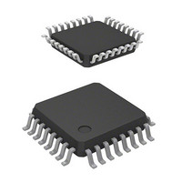
M37544G2AGP Renesas Electronics America, M37544G2AGP Datasheet - Page 9

M37544G2AGP
Manufacturer Part Number
M37544G2AGP
Description
MCU 2/5V 8K 32-LQFP
Manufacturer
Renesas Electronics America
Series
740/38000r
Specifications of M37544G2AGP
Core Processor
740
Core Size
8-Bit
Speed
8MHz
Connectivity
SIO, UART/USART
Peripherals
WDT
Number Of I /o
25
Program Memory Size
8KB (8K x 8)
Program Memory Type
QzROM
Ram Size
256 x 8
Voltage - Supply (vcc/vdd)
4 V ~ 5.5 V
Data Converters
A/D 6x8b
Oscillator Type
Internal
Operating Temperature
-20°C ~ 85°C
Package / Case
32-LQFP
Lead Free Status / RoHS Status
Contains lead / RoHS non-compliant
Eeprom Size
-
Available stocks
Company
Part Number
Manufacturer
Quantity
Price
Company:
Part Number:
M37544G2AGP#U0
Manufacturer:
TI
Quantity:
272
Company:
Part Number:
M37544G2AGP#U0
Manufacturer:
Renesas Electronics America
Quantity:
10 000
Rev.1.04
REJ03B0012-0104Z
7544 Group
PIN DESCRIPTION
Table 1 Pin description
P2
P3
P3
P3
Vcc, Vss
V
CNVss
______
RESET
X
X
P0
P0
P0
P0
P0
P1
P1
P1
P1
P1
REF
IN
OUT
0
3
0
4
7
0
1
2
3
4
0
1
2
4
/AN
/S
–P3
/INT
/INT
/CNTR
/TX
–P0
/RxD
/TxD
/S
/CNTR
____
RDY
Pin
CLK
0
OUT
3
7
1
0
–P2
1
0
2004.06.08
5
/AN
5
I/O port P2
I/O port P3
Power source
Analog reference
voltage
CNVss
Reset input
Clock input
Clock output
I/O port P0
I/O port P1
Name
page 7 of 66
•Apply voltage of 4.0 to 5.5 V to Vcc, and 0 V to Vss.
•Reference voltage input pin for A/D converter
•Chip operating mode control pin, which is always connected to Vss.
•Reset input pin for active “L”
•Input and output pins for main clock generating circuit
•Connect a ceramic resonator or quartz-crystal oscillator between the X
•For using RC oscillator, short between the X
•If an external clock is used, connect the clock source to the X
• When the on-chip oscillator is selected as the main clock, connect X
•8-bit I/O port.
•I/O direction register allows each pin to be individually pro-
•CMOS compatible input level
•CMOS 3-state output structure
•P0 can output a large current for driving LED.
•Whether a built-in pull-up resistor is to be used or not can be de-
•5-bit I/O port
•I/O direction register allows each pin to be individually pro-
•CMOS compatible input level
•CMOS 3-state output structure
•CMOS/TTL level can be switched for P1
•6-bit I/O port having almost the same function as P0
•CMOS compatible input level
•CMOS 3-state output structure
•6-bit I/O port
•I/O direction register allows each pin to be individually programmed as either input or output.
•CMOS compatible input level (CMOS/TTL level can be switched for P3
•CMOS 3-state output structure
•P3 can output a large current for driving LED.
•Whether a built-in pull-up resistor is to be used or not can be de-
grammed as either input or output.
termined by program.
grammed as either input or output.
termined by program.
0
and P1
IN
and X
Function
2
OUT
pins, and connect the capacitor and resistor.
IN
pin and leave the X
IN
• Serial I/O function pin
• Timer X function pin
• Input pins for A/D converter
• Interrupt input pins
Function expect a port function
• Key-input (key-on wake up
• Timer X and timer A function
pin to V
interrupt input) pins
pin
IN
4
and P3
and X
CC
and leave X
OUT
7
).
OUT
pins.
pin open.
OUT
open.


