M37544G2AGP Renesas Electronics America, M37544G2AGP Datasheet
M37544G2AGP
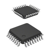
Specifications of M37544G2AGP
Available stocks


Related parts for M37544G2AGP


M37544G2AGP Summary of contents
Page 1
To our customers, Old Company Name in Catalogs and Other Documents st On April 1 , 2010, NEC Electronics Corporation merged with Renesas Technology Corporation, and Renesas Electronics Corporation took over all the business of both companies. Therefore, although the ...
Page 2
All information included in this document is current as of the date this document is issued. Such information, however, is subject to change without any prior notice. Before purchasing or using any Renesas Electronics products listed herein, please confirm ...
Page 3
Group (QzROM version) SINGLE-CHIP 8-BIT CMOS MICROCOMPUTER DESCRIPTION The 7544 Group is the 8-bit microcomputer based on the 740 fam- ily core technology. The 7544 Group has a serial interface, 8-bit timers, a 16-bit timer, and an A/D converter, ...
Page 4
... /CNTR Package type : PLQP0032GB-A (32P6U-A) Fig. 2 Pin configuration (PLQP0032GB-A type) REJ03B0108-0103 Rev.1.03 Mar 31, 2009 page CLK / RDY / / / / / / REF 11 12 CNV OUT M37544G2A-XXXGP 28 CLK 29 RDY M37544G2AGP (LED ) (LED ) (LED ) (LED ) (LED )/ OUT 25 P0 (LED ) (LED ) (LED )/CNTR (LED )/INT (LED )/INT 4 12 ...
Page 5
Group (QzROM version) P1 /CNTR / / / / / / REF RESET CNV OUT ...
Page 6
Group (QzROM version) Table 1 Performance overview Parameter Number of basic instructions Instruction execution time Oscillation frequency Memory sizes ROM RAM Input output port P0, P1, P2, P3 Interrupt Timer Serial interface A/D converter Watchdog timer Clock generating circuits ...
Page 7
Group (QzROM version) FUNCTIONAL BLOCK Fig. 4 Functional block diagram (PRDP0032BA-A package) REJ03B0108-0103 Rev.1.03 Mar 31, 2009 page ...
Page 8
Group (QzROM version) Fig. 5 Functional block diagram (PLQP0032GB-A package) REJ03B0108-0103 Rev.1.03 Mar 31, 2009 page ...
Page 9
Group (QzROM version) PIN DESCRIPTION Table 2 Pin description Name Pin Vcc, Vss Power source •Apply voltage of 1 Vcc, and Vss. V Analog reference •Reference voltage input pin for A/D converter ...
Page 10
... Fig. 6 Memory expansion plan Currently supported products are listed below. Table 3 List of supported products ROM size (bytes) Part number ROM size for User () M37544G2A-XXXSP M37544G2A-XXXGP M37544G2ASP M37544G2AGP M37544RSS REJ03B0108-0103 Rev.1.03 Mar 31, 2009 page Memory size ROM size .......................................................................... 8 K bytes RAM size ......................................................................... 256 bytes Package PRDP0032BA-A ...
Page 11
Group (QzROM version) FUNCTIONAL DESCRIPTION Central Processing Unit (CPU) The MCU uses the standard 740 family instruction set. Refer to the table of 740 family addressing modes and machine-language instructions or the SERIES 740 <SOFTWARE> USER’S MANUAL for details ...
Page 12
Group (QzROM version) Interrupt request M (S) (S) Store Return Address on Stack M (S) (S) Subroutine Execute RTS (S) Restore Return Address ( (S) ( (S) H Note : The condition to enable the ...
Page 13
Group (QzROM version) Processor status register (PS) The processor status register is an 8-bit register consisting of flags which indicate the status of the processor after an arithmetic operation. Branch operations can be performed by testing the Carry (C) ...
Page 14
Group (QzROM version) [CPU mode register] CPUM The CPU mode register contains the stack page selection bit. This register is allocated at address 003B Switching method of CPU mode register Switch the CPU mode register (CPUM) at the head ...
Page 15
Group (QzROM version) Memory Special function register (SFR) area The SFR area in the zero page contains control registers such as I/O ports and timers. RAM RAM is used for data storage and for a stack area of subroutine ...
Page 16
Group (QzROM version) Port P0 (P0) 0000 16 Port P0 direction register (P0D) 0001 16 Port P1 (P1) 0002 16 Port P1 direction register (P1D) 0003 16 0004 Port P2 (P2) 16 Port P2 direction register (P2D) 0005 16 ...
Page 17
Group (QzROM version) I/O Ports [Direction registers] PiD The I/O ports have direction registers which determine the input/ output direction of each pin. Each bit in a direction register corre- sponds to one pin, and each pin can be ...
Page 18
Group (QzROM version) Table 6 I/O port function table Pin Name Input/output P0 /CNTR I/O port P0 I/O individual bits /TX 3 OUT P0 – /RxD I/O port P1 ...
Page 19
Group (QzROM version) (1)Port P0 0 Pull-up control Direction register Port Data bus latch CNTR interrupt input 1 To key input interrupt generating circuit (3)Port P0 3 Pull-up control Direction register Data bus Port latch Timer output P0 /TX ...
Page 20
Group (QzROM version) (7) Port P1 3 Serial I/O mode selection bit Serial I/O enable bit S output enable bit RDY Direction register Data bus Port latch Serial I/O ready output (9) Ports P2 – Direction register ...
Page 21
Group (QzROM version) Termination of unused pins • Termination of common pins I/O ports: Select an input port or an output port and follow each processing method. Output ports: Open. Table 7 Termination of unused pins Pin Termination 1 ...
Page 22
Group (QzROM version) Interrupts The 7544 Group interrupts are vector interrupts with a fixed prior- ity scheme, and generated by 12 sources: 5 external, 6 internal, and 1 software. The interrupt sources, vector addresses are shown in Table 8. ...
Page 23
Group (QzROM version) Interrupt request bit Interrupt enable bit Interrupt disable flag I Fig. 17 Interrupt control • Interrupt Disable Flag The interrupt disable flag is assigned to bit 2 of the processor sta- tus register. This flag controls ...
Page 24
Group (QzROM version Fig. 18 Structure of Interrupt-related registers REJ03B0108-0103 Rev.1.03 Mar 31, 2009 page Interrupt edge selection register (INTEDGE : address 003A , initial value : 00 16 INT ...
Page 25
Group (QzROM version) • Interrupt Request Generation, Acceptance, and Handling Interrupts have the following three phases. (i) Interrupt Request Generation An interrupt request is generated by an interrupt source (ex- ternal interrupt signal input, timer underflow, etc.) and the ...
Page 26
Group (QzROM version) SYNC Address bus Data bus SYNC : CPU operation code fetch cycle SPS Fig. 20 Interrupt sequence Internal clock φ SYNC Interrupt acceptance ...
Page 27
Group (QzROM version) Key Input Interrupt (Key-On Wake-Up) A key-on wake-up interrupt request is generated by applying “L” level to any pin of port P0 that has been set to input mode. In other words generated when ...
Page 28
Group (QzROM version) Timers The 7544 Group has 3 timers: timer 1, timer A and timer X. The division ratio of every timer and prescaler is 1/(n+1) provided that the value of the timer latch or prescaler is n. ...
Page 29
Group (QzROM version) (3) Event counter mode Timer A counts signals input from the P0 Except for this, the operation in event counter mode is the same as in timer mode. The active edge of CNTR pin input signal ...
Page 30
Group (QzROM version) Timer X Timer 8-bit timer and counts the prescaler X output. When Timer X underflows, the timer X interrupt request bit is set to “1”. Prescaler 8-bit prescaler and counts ...
Page 31
Group (QzROM version Timer X mode register (TXM : address 002B Timer X operating mode bits Timer mode Pulse output mode Event counter mode 1 1 ...
Page 32
Group (QzROM version) On-chip oscillator clock RING CNTR edge switch bit P0 /CNTR 0 1 f(X )/16 IN f(X )/2 IN On-chip oscillator clock RING Timer A operation mode bit Fig. 27 Block diagram of timer 1 and timer ...
Page 33
Group (QzROM version) Serial Interface Serial I/O Serial I/O can be used as either clock synchronous or asynchro- nous (UART) serial I/O. A dedicated timer is also provided for baud rate generation ...
Page 34
Group (QzROM version) (2) Asynchronous Serial I/O (UART) Mode Clock asynchronous serial I/O mode (UART) can be selected by clearing the serial I/O mode selection bit of the serial I/O control register to “0”. Eight serial data transfer formats ...
Page 35
Group (QzROM version) [Transmit buffer register/receive buffer register (TB/RB)] 0018 16 The transmit buffer register and the receive buffer register are lo- cated at the same address. The transmit buffer is write-only and the receive buffer is read-only. If ...
Page 36
Group (QzROM version ...
Page 37
Group (QzROM version) A/D Converter The functional blocks of the A/D converter are described below. [A/D conversion register] AD The A/D conversion register is a read-only register that stores the result of A/D conversion. Do not read out this ...
Page 38
Group (QzROM version) Watchdog Timer The watchdog timer gives a means for returning to a reset status when the program fails to run on its normal loop due to a runaway. The watchdog timer consists of an 8-bit watchdog ...
Page 39
Group (QzROM version) Source clock selection (auto-switch depending on setting of CPUM) X clock IN On-chip oscillator STP Instruction function selection bit RESET Fig. 36 Block diagram of watchdog timer b7 Fig. 37 Structure of watchdog timer control register ...
Page 40
Group (QzROM version) Reset Circuit The 7544 group starts operation by the on-chip oscillator after sys- tem is released from reset. Accordingly, when the rising of power supply voltage passes 2.2V, set the reset input voltage to become below ...
Page 41
Group (QzROM version) (1) Port P0 direction register (2) Port P1 direction register (3) Port P2 direction register (4) Port P3 direction register (5) Pull-up control register (6) Port P1P3 control register (7) Serial I/O status register (8) Serial ...
Page 42
Group (QzROM version) Clock Generating Circuit An oscillation circuit can be formed by connecting a resonator be- tween X and X , and an RC oscillation circuit can be formed IN OUT by connecting a resistor and a capacitor. ...
Page 43
Group (QzROM version) (1) Oscillation control • Stop mode When the STP instruction is executed, the internal clock φ stops at an “H” level and the X oscillator stops. At this time, timer 1 is set IN to “01 ...
Page 44
Group (QzROM version) Oscillation stop detection circuit The oscillation stop detection circuit is used for reset occurrence when a ceramic resonator or an oscillation circuit stops by discon- nection. When internal reset occurs, reset because of oscillation stop can ...
Page 45
Group (QzROM version (Note) On-chip oscillator mode RING On-chip oscillator STP instruction Reset Interrupt disable flag l Interrupt request Note: Although a feed-back resistor exists on-chip, an external feed-back resistor may be needed depending ...
Page 46
Group (QzROM version) Interrupt Interrupt STP instruction State 1 Operation clock source: CPUM ← Operation clock source: f(X ) (Note 1) IN f(X ) (Note 1) IN f(X ) oscillation enabled IN f(X ) oscillation enabled IN ...
Page 47
Group (QzROM version) QzROM Writing Mode In the QzROM writing mode, the user ROM area can be rewritten while the microcomputer is mounted on-board by using a serial programmer which is applicable for this microcomputer. Table 9 lists the ...
Page 48
Group (QzROM version) ESCLK P1 P1 RESET Package type: PRDP0032BA-A (32P4B) Fig. 50 Pin connection diagram (M37544G2ASP) REJ03B0108-0103 Rev.1.03 Mar 31, 2009 page CLK 2 /S ...
Page 49
... Group (QzROM version) P0 (LED 7 ESPGMB ESDA ESCLK /CNTR Package type: PLQP0032GB-A (32P6U-A) Fig. 51 Pin connection diagram (M37544G2AGP) REJ03B0108-0103 Rev.1.03 Mar 31, 2009 page CLK M37544G2AGP 29 RDY (LED )/INT (LED ) (LED ) (LED ) (LED ) OUT Connect to oscillation circuit : QzROM pin RESET ...
Page 50
Group (QzROM version Open-collector buffer Note: For the programming circuit, the wiring capacity of each signal pin must not exceed 47 ...
Page 51
Group (QzROM version) T_VDD T_VPP T_TXD T_RXD T_SCLK T_BUSY T_PGM/OE/MD RESET circuit T_RESET GND Note: For the programming circuit, the wiring capacity of each signal pin must not exceed 47 pF. Fig. 53 When using E8 programmer, connection example ...
Page 52
Group (QzROM version) NOTES ON PROGRAMMING Processor Status Register The contents of the processor status register (PS) after reset are undefined except for the interrupt disable flag I which is “1”. After reset, initialize flags which affect program execution. ...
Page 53
Group (QzROM version) NOTES ON USE Countermeasures against noise 1. Shortest wiring length (1) Package Select the smallest possible package to make the total wiring length short. <Reason> The wiring length depends on a microcomputer package. Use of a ...
Page 54
Group (QzROM version) 2. Connection of bypass capacitor across V Connect an approximately 0.1 µ F bypass capacitor across the V line and the V line as follows: CC • Connect a bypass capacitor across the V at equal ...
Page 55
Group (QzROM version) 4. Oscillator concerns So that the product obtains the stabilized operation clock on the user system and its condition, contact the resonator manufacturer and select the resonator and oscillation circuit constants. Be careful especially when range ...
Page 56
Group (QzROM version) 5. Setup for I/O ports Setup I/O ports using hardware and software as follows: <Hardware> • Connect a resistor of 100 Ω or more to an I/O port in series. <Software> • As for an input ...
Page 57
Group (QzROM version) NOTES ON QzROM Product shipped in blank As for the product shipped in blank, Renesas does not perform the writing test to user ROM area after the assembly process though the QzROM writing test is performed ...
Page 58
Group (QzROM version) ELECTRICAL CHARACTERISTICS (QzROM version) 1.7544Group (QzROM version) Applied to: M37544G2A-XXXSP/GP, M37544G2ASP/GP Absolute Maximum Ratings Table 10 Absolute maximum ratings Symbol Parameter V Power source voltage CC V Input voltage I P0 – –P1 , ...
Page 59
Group (QzROM version) Recommended Operating Conditions Table 11 Recommended operating conditions (1) (V Symbol V Power source voltage (ceramic) CC Power source voltage (RC) Power source voltage (On-chip oscillator) V Power source voltage SS V Analog reference voltage REF ...
Page 60
Group (QzROM version) Recommended Operating Conditions (continued) Table 12 Recommended operating conditions (2) (V Symbol I “H” peak output current (Note 1) OH(peak) P0 – – – “L” peak ...
Page 61
Group (QzROM version) Electrical Characteristics Table 13 Electrical characteristics (1) (V Symbol Parameter “H” output voltage – – – “L” output voltage –P1 , ...
Page 62
Group (QzROM version) Electrical Characteristics (continued) Table 14 Electrical characteristics (2) (V Symbol Parameter I Power source High-speed mode, f(X CC current Output transistors “off” High-speed mode, V Output transistors “off” Double-speed mode, f(X Output transistors “off” Middle-speed mode, ...
Page 63
Group (QzROM version) A/D Converter Characteristics Table 15 A/D Converter characteristics (V Symbol Parameter — Resolution ABS Absolute accuracy (quantification error excluded) t Conversion time CONV R Ladder resistor LADDER I Reference power source VREF input current I A/D ...
Page 64
Group (QzROM version) Switching Characteristics Table 17 Switching characteristics (V Symbol Serial I/O clock output “H” pulse width WH CLK Serial I/O clock output “L” pulse width WL CLK t (S –TxD) Serial ...
Page 65
Group (QzROM version) CNTR 0 CNTR 1 INT , INT 0 1 RESET CLK R D (at receive (at transmit) X Fig. 66 Timing chart REJ03B0108-0103 Rev.1.03 Mar 31, 2009 page 63 of ...
Page 66
Group (QzROM version) PACKAGE OUTLINE Diagrams showing the latest package dimensions and mounting information are available in the “Packages” section of the Renesas Technology website. JEITA Package Code RENESAS Code P-SDIP32-8.9x28-1.78 PRDP0032BA SEATING PLANE ...
Page 67
Group (QzROM version) APPENDIX NOTES ON PROGRAMMING 1. Processor Status Register (1) Initializing of processor status register Flags which affect program execution must be initialized after a re- set. In particular essential to initialize the T and ...
Page 68
Group (QzROM version) 6. Read-modify-write instruction Do not execute a read-modify-write instruction to the read invalid address (SFR). The read-modify-write instruction operates in the following se- quence: read one-byte of data from memory, modify the data, write the data ...
Page 69
Group (QzROM version) Termination of Unused Pins 1. Terminate unused pins Perform the following wiring at the shortest possible distance ( less) from microcomputer pins. (1) I/O ports Set the I/O ports for the input mode and ...
Page 70
Group (QzROM version) Notes on Timers 1. When 255) is written to a timer latch, the frequency divi- sion ratio is 1/(n+1). 2. When a count source of timer X is switched, stop a count of ...
Page 71
Group (QzROM version) Notes on Serial Interface 1. Clock synchronous serial I/O (1) When the transmit operation is stopped, clear the serial I/O en- able bit (bit 7) and the transmit enable bit (bit 4 of serial I/O control ...
Page 72
Group (QzROM version) 4. I/O pin function when serial I/O is enabled. The pin functions and P1 2 CLK follows according to the setting values of a serial I/O mode selec- tion bit (bit 6 of ...
Page 73
Group (QzROM version) Notes on Clock Generating Circuit 1. Switch of ceramic/quartz-crystal oscillation and RC oscillation After releasing reset, the oscillation mode selection bit (bit 5 of CPU mode register (address 003B )) is “0” (ceramic/quartz-crys- 16 tal oscillation ...
Page 74
Group (QzROM version) Notes on Oscillation Stop Detection Circuit 1. Oscillation stop detection status bit is initialized by the following operation. (1) External reset (2) Write “0” data to the ceramic or RC oscillation stop detection function active bit. ...
Page 75
REVISION HISTORY Rev. Date Page First edition issued 1.00 Oct 26, 2004 – 1.01 Nov 24, 2004 46 Table 12 Electrical characteristics: Minimum value of V The followings are added; 48-50 - A/D Converter characteristics - Timing requirements - Switching ...
Page 76
REVISION HISTORY Rev. Date Page 1.03 Mar 31, 2009 71 Notes on Clock Generation Circuit “9. Count source” added 72 “NOTES ON QzROM” revised All trademarks and registered trademarks are the property of their respective owners. 7544 Group (QzROM version) ...
Page 77
Notes: 1. This document is provided for reference purposes only so that Renesas customers may select the appropriate Renesas products for their use. Renesas neither makes warranties or representations with respect to the accuracy or completeness of the information contained ...