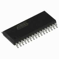
AT90PWM3-16SQ Atmel, AT90PWM3-16SQ Datasheet - Page 167

AT90PWM3-16SQ
Manufacturer Part Number
AT90PWM3-16SQ
Description
IC AVR MCU FLASH 8K 32SOIC
Manufacturer
Atmel
Series
AVR® 90PWM Lightingr
Datasheet
1.AT90PWM3B-16SU.pdf
(361 pages)
Specifications of AT90PWM3-16SQ
Core Processor
AVR
Core Size
8-Bit
Speed
16MHz
Connectivity
SPI, UART/USART
Peripherals
Brown-out Detect/Reset, POR, PWM, WDT
Number Of I /o
27
Program Memory Size
8KB (8K x 8)
Program Memory Type
FLASH
Eeprom Size
512 x 8
Ram Size
512 x 8
Voltage - Supply (vcc/vdd)
2.7 V ~ 5.5 V
Data Converters
A/D 11x10b; D/A 1x10b
Oscillator Type
Internal
Operating Temperature
-40°C ~ 105°C
Package / Case
32-SOIC (7.5mm Width)
Processor Series
AT90PWMx
Core
AVR8
Data Bus Width
8 bit
Data Ram Size
512 B
Interface Type
SPI, USART
Maximum Clock Frequency
16 MHz
Number Of Programmable I/os
27
Number Of Timers
2
Operating Supply Voltage
2.7 V to 5.5 V
Maximum Operating Temperature
+ 105 C
Mounting Style
SMD/SMT
3rd Party Development Tools
EWAVR, EWAVR-BL
Development Tools By Supplier
ATAVRDRAGON, ATSTK500, ATSTK600, ATAVRISP2, ATAVRONEKIT, ATAVRFBKIT, ATAVRISP2
Minimum Operating Temperature
- 40 C
On-chip Adc
10 bit, 11 Channel
On-chip Dac
10 bit, 1 Channel
For Use With
ATSTK600-SOIC - STK600 SOCKET/ADAPTER FOR SOICATAVRMC200 - KIT EVAL FOR AT90PWM3 ASYNCATAVRFBKIT - KIT DEMO BALLAST FOR AT90PWM2ATSTK520 - ADAPTER KIT FOR 90PWM
Lead Free Status / RoHS Status
Lead free / RoHS Compliant
- Current page: 167 of 361
- Download datasheet (7Mb)
16.25.14 PSC n Input A Control Register – PFRCnA
4317J–AVR–08/10
• Bit 7:6 – PPRE21:0 : PSC 2 Prescaler Select
This two bits select the PSC input clock division factor.All generated waveform will be modified
by this factor.
Table 16-16. PSC 2 Prescaler Selection
• Bit 5 – PBFM2 : Balance Flank Width Modulation
When this bit is clear, Flank Width Modulation operates on On-Time 1 only.
When this bit is set, Flank Width Modulation operates on On-Time 0 and On-Time 1.
• Bit 4 – PAOC2B : PSC 2 Asynchronous Output Control B
When this bit is set, Fault input selected to block B can act directly to PSCOUT21 and
PSCOUT23 outputs. See Section “PSC Clock Sources”, page 159.
• Bit 3 – PAOC2A : PSC 2 Asynchronous Output Control A
When this bit is set, Fault input selected to block A can act directly to PSCOUT20 and
PSCOUT22 outputs. See Section “PSC Clock Sources”, page 159.
• Bit 2 – PARUN2 : PSC 2 Autorun
When this bit is set, the PSC 2 starts with PSC1. That means that PSC 2 starts :
•
•
• Bit 1 – PCCYC2 : PSC 2 Complete Cycle
When this bit is set, the PSC 2 completes the entire waveform cycle before halt operation
requested by clearing PRUN2. This bit is not relevant in slave mode (PARUN2 = 1).
• Bit 0 – PRUN2 : PSC 2 Run
Writing this bit to one starts the PSC 2.
When set, this bit prevails over PARUN2 bit.
Bit
Read/Write
Initial Value
PPRE21
0
0
1
1
when PRUN1 bit in PCTL1 register is set,
or when PARUN1 bit in PCTL1 is set and PRUN0 bit in PCTL0 register is set.
PCAEnA
PPRE20
0
1
0
1
R/W
7
0
PISELnA
R/W
6
0
Description PWM2/3
No divider on PSC input clock
Divide the PSC input clock by 4
Divide the PSC input clock by 16
Divide the PSC clock by 64
PELEVnA
R/W
5
0
PFLTEnA
R/W
4
0
PRFMnA3 PRFMnA2 PRFMnA1 PRFMnA0
R/W
3
0
AT90PWM2/3/2B/3B
R/W
Description PWM2B/3B
No divider on PSC input clock
Divide the PSC input clock by 4
Divide the PSC input clock by 32
Divide the PSC clock by 256
2
0
R/W
1
0
R/W
0
0
PFRCnA
167
Related parts for AT90PWM3-16SQ
Image
Part Number
Description
Manufacturer
Datasheet
Request
R

Part Number:
Description:
IC AVR MCU FLASH 8K 32QFN
Manufacturer:
Atmel
Datasheet:

Part Number:
Description:
MCU AVR 8K FLASH 16MHZ 32-QFN
Manufacturer:
Atmel
Datasheet:

Part Number:
Description:
DEV KIT FOR AVR/AVR32
Manufacturer:
Atmel
Datasheet:

Part Number:
Description:
INTERVAL AND WIPE/WASH WIPER CONTROL IC WITH DELAY
Manufacturer:
ATMEL Corporation
Datasheet:

Part Number:
Description:
Low-Voltage Voice-Switched IC for Hands-Free Operation
Manufacturer:
ATMEL Corporation
Datasheet:

Part Number:
Description:
MONOLITHIC INTEGRATED FEATUREPHONE CIRCUIT
Manufacturer:
ATMEL Corporation
Datasheet:

Part Number:
Description:
AM-FM Receiver IC U4255BM-M
Manufacturer:
ATMEL Corporation
Datasheet:

Part Number:
Description:
Monolithic Integrated Feature Phone Circuit
Manufacturer:
ATMEL Corporation
Datasheet:

Part Number:
Description:
Multistandard Video-IF and Quasi Parallel Sound Processing
Manufacturer:
ATMEL Corporation
Datasheet:

Part Number:
Description:
High-performance EE PLD
Manufacturer:
ATMEL Corporation
Datasheet:

Part Number:
Description:
8-bit Flash Microcontroller
Manufacturer:
ATMEL Corporation
Datasheet:

Part Number:
Description:
2-Wire Serial EEPROM
Manufacturer:
ATMEL Corporation
Datasheet:


