AT90PWM3-16SQ Atmel, AT90PWM3-16SQ Datasheet - Page 123
AT90PWM3-16SQ
Manufacturer Part Number
AT90PWM3-16SQ
Description
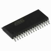
IC AVR MCU FLASH 8K 32SOIC
Manufacturer
Atmel
Series
AVR® 90PWM Lightingr
Datasheet
1.AT90PWM3B-16SU.pdf
(361 pages)
Specifications of AT90PWM3-16SQ
Core Processor
AVR
Core Size
8-Bit
Speed
16MHz
Connectivity
SPI, UART/USART
Peripherals
Brown-out Detect/Reset, POR, PWM, WDT
Number Of I /o
27
Program Memory Size
8KB (8K x 8)
Program Memory Type
FLASH
Eeprom Size
512 x 8
Ram Size
512 x 8
Voltage - Supply (vcc/vdd)
2.7 V ~ 5.5 V
Data Converters
A/D 11x10b; D/A 1x10b
Oscillator Type
Internal
Operating Temperature
-40°C ~ 105°C
Package / Case
32-SOIC (7.5mm Width)
Processor Series
AT90PWMx
Core
AVR8
Data Bus Width
8 bit
Data Ram Size
512 B
Interface Type
SPI, USART
Maximum Clock Frequency
16 MHz
Number Of Programmable I/os
27
Number Of Timers
2
Operating Supply Voltage
2.7 V to 5.5 V
Maximum Operating Temperature
+ 105 C
Mounting Style
SMD/SMT
3rd Party Development Tools
EWAVR, EWAVR-BL
Development Tools By Supplier
ATAVRDRAGON, ATSTK500, ATSTK600, ATAVRISP2, ATAVRONEKIT, ATAVRFBKIT, ATAVRISP2
Minimum Operating Temperature
- 40 C
On-chip Adc
10 bit, 11 Channel
On-chip Dac
10 bit, 1 Channel
For Use With
ATSTK600-SOIC - STK600 SOCKET/ADAPTER FOR SOICATAVRMC200 - KIT EVAL FOR AT90PWM3 ASYNCATAVRFBKIT - KIT DEMO BALLAST FOR AT90PWM2ATSTK520 - ADAPTER KIT FOR 90PWM
Lead Free Status / RoHS Status
Lead free / RoHS Compliant


4317J–AVR–08/10
I/O pin it is connected to. However, note that the Data Direction Register (DDR) bit correspond-
ing to the OCnA or OCnB pin must be set in order to enable the output driver.
When the OCnA or OCnB is connected to the pin, the function of the COMnx1:0 bits is depen-
dent of the WGMn3:0 bits setting.
WGMn3:0 bits are set to a Normal or a CTC mode (non-PWM).
Table 15-2.
Table 15-3
PWM mode.
Table 15-3.
Note:
Table 15-4
correct or the phase and frequency correct, PWM mode.
Table 15-4.
COMnA1/COMnB1
COMnA1/COMnB1
COMnA1/COMnB1
1. A special case occurs when OCRnA/OCRnB equals TOP and COMnA1/COMnB1 is set. In
0
0
1
1
0
0
1
1
0
this case the compare match is ignored, but the set or clear is done at TOP.
Mode” on page 115.
shows the COMnx1:0 bit functionality when the WGMn3:0 bits are set to the phase
shows the COMnx1:0 bit functionality when the WGMn3:0 bits are set to the fast
Compare Output Mode, non-PWM
Compare Output Mode, Fast PWM
Compare Output Mode, Phase Correct and Phase and Frequency Correct
PWM
(1)
COMnA0/COMnB0
COMnA0/COMnB0
COMnA0/COMnB0
for more details.
0
1
0
1
0
1
0
1
0
Table 15-2
Description
Normal port operation, OCnA/OCnB disconnected.
Toggle OCnA/OCnB on Compare Match.
Clear OCnA/OCnB on Compare Match (Set output to
low level).
Set OCnA/OCnB on Compare Match (Set output to
high level).
Description
Normal port operation, OCnA/OCnB disconnected.
WGMn3:0 = 14 or 15: Toggle OC1A on Compare
Match, OC1B disconnected (normal port operation).
For all other WGM1 settings, normal port operation,
OC1A/OC1B disconnected.
Clear OCnA/OCnB on Compare Match, set
OCnA/OCnB at TOP
Set OCnA/OCnB on Compare Match, clear
OCnA/OCnB at TOP
Description
Normal port operation, OCnA/OCnB disconnected.
shows the COMnx1:0 bit functionality when the
(1)
AT90PWM2/3/2B/3B
See “Fast PWM
123
Related parts for AT90PWM3-16SQ
Image
Part Number
Description
Manufacturer
Datasheet
Request
R

Part Number:
Description:
IC AVR MCU FLASH 8K 32QFN
Manufacturer:
Atmel
Datasheet:

Part Number:
Description:
MCU AVR 8K FLASH 16MHZ 32-QFN
Manufacturer:
Atmel
Datasheet:

Part Number:
Description:
DEV KIT FOR AVR/AVR32
Manufacturer:
Atmel
Datasheet:

Part Number:
Description:
INTERVAL AND WIPE/WASH WIPER CONTROL IC WITH DELAY
Manufacturer:
ATMEL Corporation
Datasheet:
Part Number:
Description:
Low-Voltage Voice-Switched IC for Hands-Free Operation
Manufacturer:
ATMEL Corporation
Datasheet:
Part Number:
Description:
MONOLITHIC INTEGRATED FEATUREPHONE CIRCUIT
Manufacturer:
ATMEL Corporation
Datasheet:
Part Number:
Description:
AM-FM Receiver IC U4255BM-M
Manufacturer:
ATMEL Corporation
Datasheet:
Part Number:
Description:
Monolithic Integrated Feature Phone Circuit
Manufacturer:
ATMEL Corporation
Datasheet:
Part Number:
Description:
Multistandard Video-IF and Quasi Parallel Sound Processing
Manufacturer:
ATMEL Corporation
Datasheet:
Part Number:
Description:
High-performance EE PLD
Manufacturer:
ATMEL Corporation
Datasheet:
Part Number:
Description:
8-bit Flash Microcontroller
Manufacturer:
ATMEL Corporation
Datasheet:
Part Number:
Description:
2-Wire Serial EEPROM
Manufacturer:
ATMEL Corporation
Datasheet: