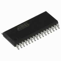
AT90PWM3-16SQ Atmel, AT90PWM3-16SQ Datasheet - Page 110

AT90PWM3-16SQ
Manufacturer Part Number
AT90PWM3-16SQ
Description
IC AVR MCU FLASH 8K 32SOIC
Manufacturer
Atmel
Series
AVR® 90PWM Lightingr
Datasheet
1.AT90PWM3B-16SU.pdf
(361 pages)
Specifications of AT90PWM3-16SQ
Core Processor
AVR
Core Size
8-Bit
Speed
16MHz
Connectivity
SPI, UART/USART
Peripherals
Brown-out Detect/Reset, POR, PWM, WDT
Number Of I /o
27
Program Memory Size
8KB (8K x 8)
Program Memory Type
FLASH
Eeprom Size
512 x 8
Ram Size
512 x 8
Voltage - Supply (vcc/vdd)
2.7 V ~ 5.5 V
Data Converters
A/D 11x10b; D/A 1x10b
Oscillator Type
Internal
Operating Temperature
-40°C ~ 105°C
Package / Case
32-SOIC (7.5mm Width)
Processor Series
AT90PWMx
Core
AVR8
Data Bus Width
8 bit
Data Ram Size
512 B
Interface Type
SPI, USART
Maximum Clock Frequency
16 MHz
Number Of Programmable I/os
27
Number Of Timers
2
Operating Supply Voltage
2.7 V to 5.5 V
Maximum Operating Temperature
+ 105 C
Mounting Style
SMD/SMT
3rd Party Development Tools
EWAVR, EWAVR-BL
Development Tools By Supplier
ATAVRDRAGON, ATSTK500, ATSTK600, ATAVRISP2, ATAVRONEKIT, ATAVRFBKIT, ATAVRISP2
Minimum Operating Temperature
- 40 C
On-chip Adc
10 bit, 11 Channel
On-chip Dac
10 bit, 1 Channel
For Use With
ATSTK600-SOIC - STK600 SOCKET/ADAPTER FOR SOICATAVRMC200 - KIT EVAL FOR AT90PWM3 ASYNCATAVRFBKIT - KIT DEMO BALLAST FOR AT90PWM2ATSTK520 - ADAPTER KIT FOR 90PWM
Lead Free Status / RoHS Status
Lead free / RoHS Compliant
- Current page: 110 of 361
- Download datasheet (7Mb)
15.5.1
15.5.2
15.5.3
15.6
110
Output Compare Units
AT90PWM2/3/2B/3B
Input Capture Trigger Source
Noise Canceler
Using the Input Capture Unit
For more information on how to access the 16-bit registers refer to
on page
The trigger sources for the Input Capture unit arethe Input Capture pin (ICP1A & ICP1B).
Be aware that changing trigger source can trigger a capture. The Input Capture Flag must there-
fore be cleared after the change.
The Input Capture pin (ICPn) IS sampled using the same technique as for the Tn pin
1 on page
enabled, additional logic is inserted before the edge detector, which increases the delay by four
system clock cycles. Note that the input of the noise canceler and edge detector is always
enabled unless the Timer/Counter is set in a Waveform Generation mode that uses ICRn to
define TOP.
An Input Capture can be triggered by software by controlling the port of the ICPn pin.
The noise canceler improves noise immunity by using a simple digital filtering scheme. The
noise canceler input is monitored over four samples, and all four must be equal for changing the
output that in turn is used by the edge detector.
The noise canceler is enabled by setting the Input Capture Noise Canceler (ICNCn) bit in
Timer/Counter Control Register B (TCCRnB). When enabled the noise canceler introduces addi-
tional four system clock cycles of delay from a change applied to the input, to the update of the
ICRn Register. The noise canceler uses the system clock and is therefore not affected by the
prescaler.
The main challenge when using the Input Capture unit is to assign enough processor capacity
for handling the incoming events. The time between two events is critical. If the processor has
not read the captured value in the ICRn Register before the next event occurs, the ICRn will be
overwritten with a new value. In this case the result of the capture will be incorrect.
When using the Input Capture interrupt, the ICRn Register should be read as early in the inter-
rupt handler routine as possible. Even though the Input Capture interrupt has relatively high
priority, the maximum interrupt response time is dependent on the maximum number of clock
cycles it takes to handle any of the other interrupt requests.
Using the Input Capture unit in any mode of operation when the TOP value (resolution) is
actively changed during operation, is not recommended.
Measurement of an external signal’s duty cycle requires that the trigger edge is changed after
each capture. Changing the edge sensing must be done as early as possible after the ICRn
Register has been read. After a change of the edge, the Input Capture Flag (ICFn) must be
cleared by software (writing a logical one to the I/O bit location). For measuring frequency only,
the clearing of the ICFn Flag is not required (if an interrupt handler is used).
The 16-bit comparator continuously compares TCNTn with the Output Compare Register
(OCRnx). If TCNT equals OCRnx the comparator signals a match. A match will set the Output
Compare Flag (OCFnx) at the next “timer clock cycle”. If enabled (OCIEnx = 1), the Output Com-
pare Flag generates an Output Compare interrupt. The OCFnx Flag is automatically cleared
when the interrupt is executed. Alternatively the OCFnx Flag can be cleared by software by writ-
104.
82). The edge detector is also identical. However, when the noise canceler is
“Accessing 16-bit Registers”
4317J–AVR–08/10
(Figure 13-
Related parts for AT90PWM3-16SQ
Image
Part Number
Description
Manufacturer
Datasheet
Request
R

Part Number:
Description:
IC AVR MCU FLASH 8K 32QFN
Manufacturer:
Atmel
Datasheet:

Part Number:
Description:
MCU AVR 8K FLASH 16MHZ 32-QFN
Manufacturer:
Atmel
Datasheet:

Part Number:
Description:
DEV KIT FOR AVR/AVR32
Manufacturer:
Atmel
Datasheet:

Part Number:
Description:
INTERVAL AND WIPE/WASH WIPER CONTROL IC WITH DELAY
Manufacturer:
ATMEL Corporation
Datasheet:

Part Number:
Description:
Low-Voltage Voice-Switched IC for Hands-Free Operation
Manufacturer:
ATMEL Corporation
Datasheet:

Part Number:
Description:
MONOLITHIC INTEGRATED FEATUREPHONE CIRCUIT
Manufacturer:
ATMEL Corporation
Datasheet:

Part Number:
Description:
AM-FM Receiver IC U4255BM-M
Manufacturer:
ATMEL Corporation
Datasheet:

Part Number:
Description:
Monolithic Integrated Feature Phone Circuit
Manufacturer:
ATMEL Corporation
Datasheet:

Part Number:
Description:
Multistandard Video-IF and Quasi Parallel Sound Processing
Manufacturer:
ATMEL Corporation
Datasheet:

Part Number:
Description:
High-performance EE PLD
Manufacturer:
ATMEL Corporation
Datasheet:

Part Number:
Description:
8-bit Flash Microcontroller
Manufacturer:
ATMEL Corporation
Datasheet:

Part Number:
Description:
2-Wire Serial EEPROM
Manufacturer:
ATMEL Corporation
Datasheet:


