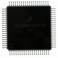
MC9S12C128CFUE Freescale Semiconductor, MC9S12C128CFUE Datasheet - Page 179

MC9S12C128CFUE
Manufacturer Part Number
MC9S12C128CFUE
Description
IC MCU 128K FLASH 25MHZ 80-QFP
Manufacturer
Freescale Semiconductor
Series
HCS12r
Specifications of MC9S12C128CFUE
Core Processor
HCS12
Core Size
16-Bit
Speed
25MHz
Connectivity
CAN, EBI/EMI, SCI, SPI
Peripherals
POR, PWM, WDT
Number Of I /o
60
Program Memory Size
128KB (128K x 8)
Program Memory Type
FLASH
Ram Size
4K x 8
Voltage - Supply (vcc/vdd)
2.35 V ~ 5.5 V
Data Converters
A/D 8x10b
Oscillator Type
Internal
Operating Temperature
-40°C ~ 85°C
Package / Case
80-QFP
Cpu Family
HCS12
Device Core Size
16b
Frequency (max)
25MHz
Interface Type
CAN/SCI/SPI
Total Internal Ram Size
4KB
# I/os (max)
60
Number Of Timers - General Purpose
8
Operating Supply Voltage (typ)
2.5/5V
Operating Supply Voltage (max)
2.75/5.5V
Operating Supply Voltage (min)
2.35/2.97V
On-chip Adc
8-chx10-bit
Instruction Set Architecture
CISC
Operating Temp Range
-40C to 85C
Operating Temperature Classification
Industrial
Mounting
Surface Mount
Pin Count
80
Package Type
PQFP
Processor Series
S12C
Core
HCS12
Data Bus Width
16 bit
Data Ram Size
4000 B
Maximum Clock Frequency
25 MHz
Number Of Programmable I/os
61
Number Of Timers
1
Operating Supply Voltage
- 0.3 V to + 6.5 V
Maximum Operating Temperature
+ 85 C
Mounting Style
SMD/SMT
3rd Party Development Tools
EWHCS12
Development Tools By Supplier
M68EVB912C32EE
Minimum Operating Temperature
- 40 C
Lead Free Status / RoHS Status
Lead free / RoHS Compliant
Eeprom Size
-
Lead Free Status / Rohs Status
Compliant
Available stocks
Company
Part Number
Manufacturer
Quantity
Price
Company:
Part Number:
MC9S12C128CFUE
Manufacturer:
ST
Quantity:
6 246
Company:
Part Number:
MC9S12C128CFUE
Manufacturer:
Freescale Semiconductor
Quantity:
10 000
- Current page: 179 of 690
- Download datasheet (4Mb)
6.4.6
The BDM communicates with external devices serially via the BKGD pin. During reset, this pin is a mode
select input which selects between normal and special modes of operation. After reset, this pin becomes
the dedicated serial interface pin for the BDM.
The BDM serial interface is timed using the clock selected by the CLKSW bit in the status register see
Section 6.3.2.1, “BDM Status Register
the following explanation.
The BDM serial interface uses a clocking scheme in which the external host generates a falling edge on
the BKGD pin to indicate the start of each bit time. This falling edge is sent for every bit whether data is
transmitted or received. Data is transferred most significant bit (MSB) first at 16 target clock cycles per
bit. The interface times out if 512 clock cycles occur between falling edges from the host.
The BKGD pin is a pseudo open-drain pin and has an weak on-chip active pull-up that is enabled at all
times. It is assumed that there is an external pull-up and that drivers connected to BKGD do not typically
drive the high level. Because R-C rise time could be unacceptably long, the target system and host provide
brief driven-high (speedup) pulses to drive BKGD to a logic 1. The source of this speedup pulse is the host
for transmit cases and the target for receive cases.
The timing for host-to-target is shown in
9. All four cases begin when the host drives the BKGD pin low to generate a falling edge. Because the host
and target are operating from separate clocks, it can take the target system up to one full clock cycle to
recognize this edge. The target measures delays from this perceived start of the bit time while the host
measures delays from the point it actually drove BKGD low to start the bit up to one target clock cycle
Freescale Semiconductor
HARDWARE
HARDWARE
FIRMWARE
FIRMWARE
TRACE
WRITE
WRITE
READ
READ
GO,
BDM Serial Interface
AT ∼16 TC/BIT
COMMAND
COMMAND
COMMAND
COMMAND
COMMAND
8 BITS
DELAY
44-BC
DELAY
64-BC
AT ∼16 TC/BIT
Figure 6-6. BDM Command Structure
ADDRESS
ADDRESS
16 BITS
DATA
MC9S12C-Family / MC9S12GC-Family
COMMAND
(BDMSTS).” This clock will be referred to as the target clock in
NEXT
DATA
Figure 6-7
Rev 01.24
DELAY
32-BC
and that of target-to-host in
Chapter 6 Background Debug Module (BDMV4) Block Description
150-BC
DELAY
COMMAND
COMMAND
NEXT
NEXT
DATA
AT ∼16 TC/BIT
16 BITS
DATA
BC = BUS CLOCK CYCLES
TC = TARGET CLOCK CYCLES
150-BC
DELAY
Figure 6-8
COMMAND
COMMAND
NEXT
NEXT
and
Figure 6-
179
Related parts for MC9S12C128CFUE
Image
Part Number
Description
Manufacturer
Datasheet
Request
R
Part Number:
Description:
Manufacturer:
Freescale Semiconductor, Inc
Datasheet:
Part Number:
Description:
Manufacturer:
Freescale Semiconductor, Inc
Datasheet:
Part Number:
Description:
Manufacturer:
Freescale Semiconductor, Inc
Datasheet:
Part Number:
Description:
Manufacturer:
Freescale Semiconductor, Inc
Datasheet:
Part Number:
Description:
Manufacturer:
Freescale Semiconductor, Inc
Datasheet:
Part Number:
Description:
Manufacturer:
Freescale Semiconductor, Inc
Datasheet:
Part Number:
Description:
Manufacturer:
Freescale Semiconductor, Inc
Datasheet:
Part Number:
Description:
Manufacturer:
Freescale Semiconductor, Inc
Datasheet:
Part Number:
Description:
Manufacturer:
Freescale Semiconductor, Inc
Datasheet:
Part Number:
Description:
Manufacturer:
Freescale Semiconductor, Inc
Datasheet:
Part Number:
Description:
Manufacturer:
Freescale Semiconductor, Inc
Datasheet:
Part Number:
Description:
Manufacturer:
Freescale Semiconductor, Inc
Datasheet:
Part Number:
Description:
Manufacturer:
Freescale Semiconductor, Inc
Datasheet:
Part Number:
Description:
Manufacturer:
Freescale Semiconductor, Inc
Datasheet:
Part Number:
Description:
Manufacturer:
Freescale Semiconductor, Inc
Datasheet:


