MC9S12C128CFUE Freescale Semiconductor, MC9S12C128CFUE Datasheet - Page 161
MC9S12C128CFUE
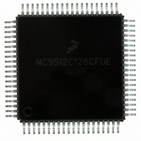
Manufacturer Part Number
MC9S12C128CFUE
Description
IC MCU 128K FLASH 25MHZ 80-QFP
Manufacturer
Freescale Semiconductor
Series
HCS12r
Specifications of MC9S12C128CFUE
Core Processor
HCS12
Core Size
16-Bit
Speed
25MHz
Connectivity
CAN, EBI/EMI, SCI, SPI
Peripherals
POR, PWM, WDT
Number Of I /o
60
Program Memory Size
128KB (128K x 8)
Program Memory Type
FLASH
Ram Size
4K x 8
Voltage - Supply (vcc/vdd)
2.35 V ~ 5.5 V
Data Converters
A/D 8x10b
Oscillator Type
Internal
Operating Temperature
-40°C ~ 85°C
Package / Case
80-QFP
Cpu Family
HCS12
Device Core Size
16b
Frequency (max)
25MHz
Interface Type
CAN/SCI/SPI
Total Internal Ram Size
4KB
# I/os (max)
60
Number Of Timers - General Purpose
8
Operating Supply Voltage (typ)
2.5/5V
Operating Supply Voltage (max)
2.75/5.5V
Operating Supply Voltage (min)
2.35/2.97V
On-chip Adc
8-chx10-bit
Instruction Set Architecture
CISC
Operating Temp Range
-40C to 85C
Operating Temperature Classification
Industrial
Mounting
Surface Mount
Pin Count
80
Package Type
PQFP
Processor Series
S12C
Core
HCS12
Data Bus Width
16 bit
Data Ram Size
4000 B
Maximum Clock Frequency
25 MHz
Number Of Programmable I/os
61
Number Of Timers
1
Operating Supply Voltage
- 0.3 V to + 6.5 V
Maximum Operating Temperature
+ 85 C
Mounting Style
SMD/SMT
3rd Party Development Tools
EWHCS12
Development Tools By Supplier
M68EVB912C32EE
Minimum Operating Temperature
- 40 C
Lead Free Status / RoHS Status
Lead free / RoHS Compliant
Eeprom Size
-
Lead Free Status / Rohs Status
Compliant
Available stocks
Company
Part Number
Manufacturer
Quantity
Price
Company:

Part Number:
MC9S12C128CFUE
Manufacturer:
ST
Quantity:
6 246
Company:
Part Number:
MC9S12C128CFUE
Manufacturer:
Freescale Semiconductor
Quantity:
10 000


5.3.2.3
Read: Anytime
Write: Only if I mask in CCR = 1
5.4
The interrupt sub-block processes all exception requests made by the CPU. These exceptions include
interrupt vector requests and reset vector requests. Each of these exception types and their overall priority
level is discussed in the subsections below.
Freescale Semiconductor
Module Base + 0x001F
Starting address location affected by INITRG register setting.
PSEL[7:1]
INT[E:0]
Reset
Field
Field
7:0
7:1
W
R
Functional Description
PSEL7
Interrupt TEST Bits — These registers are used in special modes for testing the interrupt logic and priority
independent of the system configuration. Each bit is used to force a specific interrupt vector by writing it to a
logic 1 state. Bits are named INTE through INT0 to indicate vectors 0xFFxE through 0xFFx0. These bits can be
written only in special modes and only with the WRTINT bit set (logic 1) in the interrupt test control register
(ITCR). In addition, I interrupts must be masked using the I bit in the CCR. In this state, the interrupt input lines
to the interrupt sub-block will be disconnected and interrupt requests will be generated only by this register.
These bits can also be read in special modes to view that an interrupt requested by a system block (such as a
peripheral block) has reached the INT module.
There is a test register implemented for every eight interrupts in the overall system. All of the test registers share
the same address and are individually selected using the value stored in the ADR[3:0] bits of the interrupt test
control register (ITCR).
Note: When ADR[3:0] have the value of 0x000F, only bits 2:0 in the ITEST register will be accessible. That is,
Highest Priority I Interrupt Select Bits — The state of these bits determines which I-bit maskable interrupt will
be promoted to highest priority (of the I-bit maskable interrupts). To promote an interrupt, the user writes the least
significant byte of the associated interrupt vector address to this register. If an unimplemented vector address or
a non I-bit masked vector address (value higher than 0x00F2) is written, IRQ (0xFFF2) will be the default highest
priority interrupt.
Highest Priority I Interrupt (Optional)
1
7
vectors higher than 0xFFF4 cannot be tested using the test registers and bits 7:3 will always read as a
logic 0. If ADR[3:0] point to an unimplemented test register, writes will have no effect and reads will always
return a logic 0 value.
= Unimplemented or Reserved
PSEL6
Figure 5-4. Highest Priority I Interrupt Register (HPRIO)
1
6
Table 5-4. HPRIO Field Descriptions
Table 5-3. ITEST Field Descriptions
PSEL5
MC9S12C-Family / MC9S12GC-Family
1
5
PSEL4
Rev 01.24
1
4
Description
Description
PSEL3
0
3
Chapter 5 Interrupt (INTV1) Block Description
PSEL2
0
2
PSEL1
1
1
0
0
0
161
Related parts for MC9S12C128CFUE
Image
Part Number
Description
Manufacturer
Datasheet
Request
R

Part Number:
Description:
Manufacturer:
Freescale Semiconductor, Inc
Datasheet:
Part Number:
Description:
Manufacturer:
Freescale Semiconductor, Inc
Datasheet:
Part Number:
Description:
Manufacturer:
Freescale Semiconductor, Inc
Datasheet:
Part Number:
Description:
Manufacturer:
Freescale Semiconductor, Inc
Datasheet:
Part Number:
Description:
Manufacturer:
Freescale Semiconductor, Inc
Datasheet:
Part Number:
Description:
Manufacturer:
Freescale Semiconductor, Inc
Datasheet:
Part Number:
Description:
Manufacturer:
Freescale Semiconductor, Inc
Datasheet:
Part Number:
Description:
Manufacturer:
Freescale Semiconductor, Inc
Datasheet:
Part Number:
Description:
Manufacturer:
Freescale Semiconductor, Inc
Datasheet:
Part Number:
Description:
Manufacturer:
Freescale Semiconductor, Inc
Datasheet:
Part Number:
Description:
Manufacturer:
Freescale Semiconductor, Inc
Datasheet:
Part Number:
Description:
Manufacturer:
Freescale Semiconductor, Inc
Datasheet:
Part Number:
Description:
Manufacturer:
Freescale Semiconductor, Inc
Datasheet:
Part Number:
Description:
Manufacturer:
Freescale Semiconductor, Inc
Datasheet:
Part Number:
Description:
Manufacturer:
Freescale Semiconductor, Inc
Datasheet: