PG103003 Microchip Technology, PG103003 Datasheet - Page 12
PG103003
Manufacturer Part Number
PG103003
Description
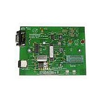
KIT PROGRAMMERS MICROID 13.56MHZ
Manufacturer
Microchip Technology
Series
MicroID®r
Type
MicroID®r
Datasheet
1.PG103003.pdf
(22 pages)
Specifications of PG103003
Contents
Programmer, Power Supply, Cable(s) and Software
Product
RFID Kits
Lead Free Status / RoHS Status
Lead free / RoHS Compliant
For Use With/related Products
MCRF355, MCRF360
Lead Free Status / RoHS Status
Lead free / RoHS Compliant, Lead free / RoHS Compliant


MCRF355
5.0
Every die on the wafer is electrically tested according
to the data sheet specifications and visually inspected
to detect any mechanical damage, such as mechanical
cracks and scratches.
Any failed die in the test or visual inspection is identified
by black colored ink. Therefore, any die covered with
black ink should not be used.
The ink dot specification:
• Ink dot size: 254 m in circular diameter
• Position: central third of die
• Color: black
• Wafer map files are also available upon request
6.0
The wafer is shipped with the following information:
• Microchip Technology Inc. MP Code
• Lot Number
• Total number of wafers in the container
• Total number of good dice in the container
• Average die per wafer (DPW)
• Scribe number of wafers with number of good
• Wafer map files are also available upon request
DS21287G-page 12
dice
FAILED DIE IDENTIFICATION
WAFER DELIVERY
DOCUMENTATION
7.0
The device is very susceptible to Electro-Static
Discharge (ESD), which can cause critical damage to
the device. Special attention is needed during the han-
dling process.
Any ultraviolet (UV) light can erase the memory cell
contents of an unpackaged device. Fluorescent lights
and sunlight can also erase the memory cell, although
it takes more time than UV lamps. Therefore, keep any
unpackaged device out of UV light and also avoid direct
exposure of strong fluorescent lights and shining
sunlight.
Certain IC manufacturing, COB and tag assembly
operations may use UV light. Operations such as back-
grind de-tape, certain cleaning procedures, epoxy or
glue cure should be done without exposing the die
surface to UV light.
Using X-ray for die inspection will not harm the die, nor
erase memory cell contents.
8.0
It is recommended that the reader reference the
following documents.
1.
2.
3.
4.
5.
“Antenna Circuit Design for RFID Applications”,
AN710, DS00710.
“RFID Tag and COB Development Guide with
Microchip’s RFID Devices”, AN830, DS00830.
“MCRF355/360 Application Note: Mode of
Operation and External Resonance Circuit”,
AN707, DS00707.
“Microchip Development Kit Sample Format for
the MCRF355/360 Devices”, TB031, DS91031.
“MCRF355/360 Reader Reference Design”,
DS21311.
NOTICE ON DIE AND WAFER
HANDLING
REFERENCES
© 2005 Microchip Technology Inc.
Related parts for PG103003
Image
Part Number
Description
Manufacturer
Datasheet
Request
R

Part Number:
Description:
Manufacturer:
Microchip Technology Inc.
Datasheet:
Part Number:
Description:
Manufacturer:
Microchip Technology Inc.
Datasheet:
Part Number:
Description:
Manufacturer:
Microchip Technology Inc.
Datasheet:
Part Number:
Description:
Manufacturer:
Microchip Technology Inc.
Datasheet:
Part Number:
Description:
Manufacturer:
Microchip Technology Inc.
Datasheet:
Part Number:
Description:
Manufacturer:
Microchip Technology Inc.
Datasheet:
Part Number:
Description:
Manufacturer:
Microchip Technology Inc.
Datasheet:
Part Number:
Description:
Manufacturer:
Microchip Technology Inc.
Datasheet: