EVAL6599-400W-S STMicroelectronics, EVAL6599-400W-S Datasheet - Page 5
EVAL6599-400W-S
Manufacturer Part Number
EVAL6599-400W-S
Description
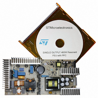
DEMO BOARD FOR L6599
Manufacturer
STMicroelectronics
Type
Power Factor Correctionr
Specifications of EVAL6599-400W-S
Main Purpose
AC/DC, Primary Side and PFC
Outputs And Type
3, Isolated
Power - Output
400W
Voltage - Output
200V, 5V, 3.3V
Current - Output
2A, 1A, 700mA
Voltage - Input
90 ~ 264VAC
Regulator Topology
Resonant
Board Type
Fully Populated
Utilized Ic / Part
L6563, L6599
Input Voltage
90 V to 264 V
Output Voltage
3.3 V to 200 V
Dimensions
132 mm x 265 mm
Product
Power Management Modules
Lead Free Status / RoHS Status
Lead free / RoHS Compliant
For Use With/related Products
L6599
Other names
497-5856
Available stocks
Company
Part Number
Manufacturer
Quantity
Price


AN2492
Main characteristics and circuit description
feedback signal in order to regulate the output voltages against load and input voltage
variations.
The main features of the L6599 are a non-linear soft-start, a current protection mode used
to program the hiccup mode timing, a dedicated pin for sequencing or brown-out (LINE) and
a stand-by pin (STBY) for burst mode operation at light loads (not used in this design).
The transformer (T1) uses the magnetic integration approach, incorporating the resonant
series and shunt inductances of the LLC resonant tank. Thus, no additional external coils
are needed for the resonance. For a detailed analysis of the LLC resonant converter, please
refer to the application note AN2450.
The secondary side power circuit is configured with a single-ended transformer winding and
full-bridge rectification (diodes D8A, D8B, D10A, D10B), which is more suitable for the
current design. In fact, with this configuration, the total junction capacitance of the output
diodes reflected at primary side is one half the capacitance in case of center-tap
transformer. This capacitance at transformer primary side may affect the behavior of the
resonant tank, changing the circuit from LLC to LLCC type, with the risk that the converter,
in light-load/no-load condition (when the feedback loop increases the operating frequency)
can no longer control the output voltage. If the converter has to operate down to zero load,
this capacitance needs to be minimized. An inherent advantage of the full-bridge
rectification is that the voltage rating of the output diodes in this configuration is one half the
rating necessary for center-tap and two diodes circuit, which translates into a lower junction
capacitance device, with consequent lower reflected capacitance at primary side.
The feedback loop is implemented by means of a classical configuration using a TL431 (U4)
to adjust the current in the optocoupler diode (U3). The optocoupler transistor modulates the
current from controller Pin 4, so the frequency will change accordingly, thus achieving the
output voltage regulation. Resistors R46 and R54 set the maximum operating frequency. In
case of a short circuit, the current entering the primary winding is detected by the lossless
circuit (C34, C39, D11, D12, R43, and R45) and the resulting signal is fed into L6599 Pin 6.
In case of overload, the voltage on Pin 6 will exceed an internal threshold that triggers a
protection sequence via Pin 2, keeping the current flowing in the circuit at a safe level.
The third stage is a small flyback converter based on the VIPer12A, a current mode
controller with integrated Power MOSFET, capable of delivering about 7 W total output
power on the output voltages (5 V and 3.3 V). The regulated output voltage is the 3.3 V
output and, also in this case, the feedback loop uses the TL431 (U7) and optocoupler (U6)
to control the output voltage. This converter is able to operate in the whole mains voltage
range, even when the PFC stage is not working. From the auxiliary winding on the primary
side of the flyback transformer (T2), a voltage Vs is available, intended to supply the other
controllers (L6563 and L6599) in addition to the VIPer12A itself.
The PFC stage and the resonant converter can be switched on and off through the circuit
based mainly on components Q7, Q8, D22 and U8, which, depending on the level of the
signal ST-BY, supplies or removes the auxiliary voltage (VAUX) necessary to start up the
controllers of the PFC and resonant stages. When the AC input voltage is applied to the
power supply, the small flyback converter switches on first. Then, when the ST-BY signal is
low, the PFC pre-regulator becomes operative, and the resonant converter can deliver the
output power to the load. Note that if Pin 9 of Connector J3 is left floating (no signal ST-BY
present), the PFC and resonant converter will not operate, and only +5 V and +3.3 V
supplies are available on the output. In order to enable the +200 V output, Pin 9 of
Connector J3 must be pulled down to ground.
5/35
Related parts for EVAL6599-400W-S
Image
Part Number
Description
Manufacturer
Datasheet
Request
R

Part Number:
Description:
EVAL BOARD FOR L6599
Manufacturer:
STMicroelectronics
Datasheet:

Part Number:
Description:
EVAL BOARD FOR L6599
Manufacturer:
STMicroelectronics
Datasheet:

Part Number:
Description:
DEMO BOARD FOR L6599
Manufacturer:
STMicroelectronics
Datasheet:

Part Number:
Description:
STMicroelectronics [RIPPLE-CARRY BINARY COUNTER/DIVIDERS]
Manufacturer:
STMicroelectronics
Datasheet:
Part Number:
Description:
STMicroelectronics [LIQUID-CRYSTAL DISPLAY DRIVERS]
Manufacturer:
STMicroelectronics
Datasheet:

Part Number:
Description:
BOARD EVAL FOR MEMS SENSORS
Manufacturer:
STMicroelectronics
Datasheet:
Part Number:
Description:
NPN TRANSISTOR POWER MODULE
Manufacturer:
STMicroelectronics
Datasheet:
Part Number:
Description:
TURBOSWITCH ULTRA-FAST HIGH VOLTAGE DIODE
Manufacturer:
STMicroelectronics
Datasheet:
Part Number:
Description:
Manufacturer:
STMicroelectronics
Datasheet:
Part Number:
Description:
DIODE / SCR MODULE
Manufacturer:
STMicroelectronics
Datasheet:
Part Number:
Description:
DIODE / SCR MODULE
Manufacturer:
STMicroelectronics
Datasheet:
Part Number:
Description:
Search -----> STE16N100
Manufacturer:
STMicroelectronics
Datasheet: