EVAL-AD5390EB Analog Devices Inc, EVAL-AD5390EB Datasheet - Page 8
EVAL-AD5390EB
Manufacturer Part Number
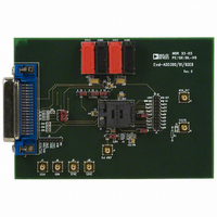
EVAL-AD5390EB
Description
BOARD EVAL FOR AD5390
Manufacturer
Analog Devices Inc
Specifications of EVAL-AD5390EB
Number Of Dac's
16
Number Of Bits
14
Outputs And Type
16, Single Ended
Sampling Rate (per Second)
125k
Data Interface
Serial
Settling Time
8µs
Dac Type
Voltage
Voltage Supply Source
Single
Operating Temperature
-40°C ~ 85°C
Utilized Ic / Part
AD5390
Lead Free Status / RoHS Status
Contains lead / RoHS non-compliant


AD5390/AD5391/AD5392
Parameter
POWER REQUIREMENTS
1
2
3
4
AD539x-3 products are calibrated with a 1.25 V reference. Temperature range for all versions: −40°C to +85°C.
Guaranteed by characterization, not production tested.
Programmable either to 1.25 V typical or 2.5 V typical via the AD539x control register. Operating the AD539x-3 products with a reference of 2.5 V leads to a
degradation in performance accuracy.
Accuracy guaranteed from VOUT = 39 mV to AV
Logic Outputs (BUSY, SDO)
Logic Output (SDA)
AV
DV
Power Supply Sensitivity
∆Midscale/∆AV
AI
AI
DI
AI
DI
Power Dissipation
DD
DD
DD
DD
DD
Output Low Voltage
Output High Voltage
High Impedance Leakage Current
High Impedance Output
Capacitance
V
Three-State Leakage Current
Three-State Output
Capacitance
DD
DD
OL
(Power-Down)
(Power-Down)
, Output Low Voltage
DD
2
2
2
AD5390-3
AD5392-3
0.4
DV
DV
±1
5
0.4
0.6
±1
8
2.7/3.6
2.7/5.5
−85
0.375
0.475
1
1
20
21
12
DD
− 50 mV.
DD
DD
− 0.5
− 0.1
1
1
AD5391-3
0.4
DV
DV
±1
5
0.4
0.6
±1
8
2.7/3.6
2.7/5.5
−85
0.375
0.475
1
1
20
21
12
DD
DD
Rev. C | Page 8 of 40
− 0.5
− 0.1
1
Unit
V max
V min
V min
μA max
pF typ
V max
V max
μA max
pF typ
V min/max
V min/max
dB typ
mA/channel
max
mA/channel
max
mA max
μA max
μA max
mW max
mW max
Test Conditions/Comments
DV
DV
DV
I
I
Outputs unloaded, boost off,
0.25 mA/channel typ
Outputs unloaded, boost on,
0.325 mA/channel typ
V
AD5390/AD5391 with outputs unloaded,
AV
AD5392 with outputs unloaded,
AV
SINK
SINK
IH
DD
DD
DD
DD
DD
= DV
= 3 mA
= 6 mA
= DV
= DV
= 2.7 V to 3.6 V, SDO only, sourcing 200 μA
= 4.5 V to 5.5 V, SDO only, sourcing 200 μA
= 2.7 V to 5.5 V, sinking 200 μA
DD
, V
DD
DD
IL
= 3 V, boost off
= 3 V, boost off
= DGND
Related parts for EVAL-AD5390EB
Image
Part Number
Description
Manufacturer
Datasheet
Request
R

Part Number:
Description:
ENERCHIP CC EVAL KIT
Manufacturer:
Cymbet Corporation
Datasheet:

Part Number:
Description:
BOARD EVAL FOR AD976
Manufacturer:
Analog Devices Inc
Datasheet:

Part Number:
Description:
BOARD EVAL FOR ADXL345
Manufacturer:
Analog Devices Inc
Datasheet:

Part Number:
Description:
ENERCHIP CC SEH EVAL KIT
Manufacturer:
Cymbet Corporation
Datasheet:

Part Number:
Description:
ENERCHIP EP ENERGY HARVEST EVAL
Manufacturer:
Cymbet Corporation
Datasheet:

Part Number:
Description:
EVAL BOARD FOR TW6864-LB2-GR
Manufacturer:
Intersil
Datasheet:
Part Number:
Description:
EVAL BOARD FOR TW8816-LB3-GR
Manufacturer:
Intersil
Datasheet:
Part Number:
Description:
EVAL BOARD FOR TW8817-TA3-GRS
Manufacturer:
Intersil
Datasheet:

Part Number:
Description:
EVALUATION MODULE FOR ADUM4160
Manufacturer:
Analog Devices Inc
Datasheet:

Part Number:
Description:
BOARD EVALUATION ADCMP581BCP
Manufacturer:
Analog Devices Inc
Datasheet:
Part Number:
Description:
BOARD EVALUATION ADM1041
Manufacturer:
Analog Devices Inc
Datasheet:

Part Number:
Description:
EVAL BOARD FOR STM32F107VCT
Manufacturer:
STMicroelectronics
Datasheet:
Part Number:
Description:
BOARD EVAL FOR AD1954
Manufacturer:
Analog Devices Inc
Datasheet:
Part Number:
Description:
BOARD EVAL FOR AD1955
Manufacturer:
Analog Devices Inc
Datasheet:

Part Number:
Description:
BOARD EVAL FOR AD7655
Manufacturer:
Analog Devices Inc
Datasheet: