EVAL-AD9831EB Analog Devices Inc, EVAL-AD9831EB Datasheet - Page 2
EVAL-AD9831EB
Manufacturer Part Number
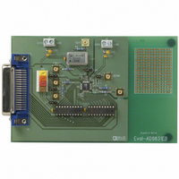
EVAL-AD9831EB
Description
BOARD EVAL FOR AD9831
Manufacturer
Analog Devices Inc
Type
Direct Digital Synthesis (DDS)r
Datasheet
1.EVAL-AD9831EB.pdf
(16 pages)
Specifications of EVAL-AD9831EB
Contents
Evaluation Board
For Use With/related Products
AD9831
Lead Free Status / RoHS Status
Contains lead / RoHS non-compliant


Parameter
SIGNAL DAC SPECIFICATIONS
DDS SPECIFICATIONS
VOLTAGE REFERENCE
LOGIC INPUTS
POWER SUPPLIES
NOTES
1
2
3
4
5
6
Specifications subject to change without notice.
AD9831–SPECIFICATIONS
Operating temperature range is as follows: A Version: –40 C to +85 C.
100% production tested.
f
See Figure 11. To reduce the wake-up time at low power supplies and low temperature, the use of an external reference is suggested.
Measured with the digital inputs static and equal to 0 V or DVDD.
The Low Power Sleep Mode current is typically 2 mA when a 1 M
The AD9831 is tested with a capacitive load of 50 pF. The part can be operated with higher capacitive loads, but the magnitude of the analog output will be attenu-
ated. For example, a 5 MHz output signal will be attenuated by 3 dB when the load capacitance equals 85 pF.
MCLK
Resolution
Update Rate (f
I
Output Compliance
DC Accuracy
Dynamic Specifications
Internal Reference @ +25 C
REFIN Input Impedance
Reference TC
REFOUT Output Impedance
V
V
I
C
AVDD
DVDD
I
I
I
Low Power Sleep Mode
OUT
INH
AA
DD
AA
INH
INL
IN
Integral Nonlinearity
Differential Nonlinearity
Signal to Noise Ratio
Total Harmonic Distortion
Spurious Free Dynamic Range (SFDR)
Clock Feedthrough
Wake-Up Time
Powerdown Option
T
= 6.25 MHz, Frequency Word = 5671C71C HEX, f
, Input Capacitance
+ I
MIN
, Input Current
Narrow Band ( 50 kHz)
Wide Band ( 2 MHz)
, Input Low Voltage
, Input High Voltage
Full Scale
DD
to T
5
MAX
MAX
4
)
2
6
Figure 1. Test Circuit with Which Specifications Are Tested
3
10nF
AD9831A
10
25
4
5
1.5
50
–53
–72
–70
–50
–60
1
Yes
1.21
1.21
10
100
300
V
0.9
10
10
2.97/5.5
2.97/5.5
12
2.5 + 0.33/MHz
15
24
1
OUT
REFERENCE
12
1
0.5
ON-BOARD
DD
= 2.11 MHz.
1
– 0.9
REFOUT
ROM
SIN
(V
REFOUT; R
7%
DD
resistor is not tied between REFOUT and AGND.
= +3.3 V
FULL-SCALE
CONTROL
10-BIT DAC
REFIN
AD9831
SET
–2–
Units
Bits
MSPS nom
mA nom
mA max
V max
LSB typ
LSB typ
dB min
dBc max
dBc min
dBc min
dBc min
dBc typ
ms typ
Volts typ
Volts min/max
M typ
ppm/ C typ
V min
V max
pF max
V min/V max
V min/V max
mA max
mA typ
mA max
mA max
mA max
= 3.9 k ; R
A max
typ
FS
ADJUST
3.9k
R
10%; +5 V
SET
COMP
IOUT
LOAD
AVDD
= 300
300
10%; AGND = DGND = 0 V; T
Test Conditions/Comments
f
f
f
5 V Power Supply
3 V Power Supply
5 V Power Supply
5 V Power Supply
3 V Power Supply
5 V Power Supply
1 M Resistor Tied Between REFOUT and AGND
10nF
MCLK
MCLK
MCLK
50pF
= 25 MHz, f
= 25 MHz, f
= 6.25 MHz, f
for IOUT unless otherwise noted)
OUT
OUT
OUT
= 1 MHz
= 1 MHz
= 2.11 MHz
A
= T
MIN
to T
MAX
; REFIN =
REV. A
Related parts for EVAL-AD9831EB
Image
Part Number
Description
Manufacturer
Datasheet
Request
R

Part Number:
Description:
ENERCHIP CC EVAL KIT
Manufacturer:
Cymbet Corporation
Datasheet:

Part Number:
Description:
BOARD EVAL FOR AD976
Manufacturer:
Analog Devices Inc
Datasheet:

Part Number:
Description:
BOARD EVAL FOR ADXL345
Manufacturer:
Analog Devices Inc
Datasheet:

Part Number:
Description:
ENERCHIP CC SEH EVAL KIT
Manufacturer:
Cymbet Corporation
Datasheet:

Part Number:
Description:
ENERCHIP EP ENERGY HARVEST EVAL
Manufacturer:
Cymbet Corporation
Datasheet:

Part Number:
Description:
EVAL BOARD FOR TW6864-LB2-GR
Manufacturer:
Intersil
Datasheet:
Part Number:
Description:
EVAL BOARD FOR TW8816-LB3-GR
Manufacturer:
Intersil
Datasheet:
Part Number:
Description:
EVAL BOARD FOR TW8817-TA3-GRS
Manufacturer:
Intersil
Datasheet:

Part Number:
Description:
EVALUATION MODULE FOR ADUM4160
Manufacturer:
Analog Devices Inc
Datasheet:

Part Number:
Description:
BOARD EVALUATION ADCMP581BCP
Manufacturer:
Analog Devices Inc
Datasheet:
Part Number:
Description:
BOARD EVALUATION ADM1041
Manufacturer:
Analog Devices Inc
Datasheet:

Part Number:
Description:
EVAL BOARD FOR STM32F107VCT
Manufacturer:
STMicroelectronics
Datasheet:
Part Number:
Description:
BOARD EVAL FOR AD1954
Manufacturer:
Analog Devices Inc
Datasheet:
Part Number:
Description:
BOARD EVAL FOR AD1955
Manufacturer:
Analog Devices Inc
Datasheet:

Part Number:
Description:
BOARD EVAL FOR AD7655
Manufacturer:
Analog Devices Inc
Datasheet: