EVAL-AD9831EB Analog Devices Inc, EVAL-AD9831EB Datasheet - Page 12
EVAL-AD9831EB
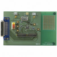
Manufacturer Part Number
EVAL-AD9831EB
Description
BOARD EVAL FOR AD9831
Manufacturer
Analog Devices Inc
Type
Direct Digital Synthesis (DDS)r
Datasheet
1.EVAL-AD9831EB.pdf
(16 pages)
Specifications of EVAL-AD9831EB
Contents
Evaluation Board
For Use With/related Products
AD9831
Lead Free Status / RoHS Status
Contains lead / RoHS non-compliant


AD9831
APPLICATIONS
The AD9831 contains functions which make it suitable for
modulation applications. The part can be used to perform
simple modulation such as FSK. More complex modulation
schemes such as GMSK and QPSK can also be implemented
using the AD9831. In an FSK application, the two frequency
registers of the AD9831 are loaded with different values; one
frequency will represent the space frequency while the other will
represent the mark frequency. The digital data stream is fed to
the FSELECT pin which will cause the AD9831 to modulate
the carrier frequency between the two values.
The AD9831 has four phase registers; this enables the part to
perform PSK. With phase shift keying, the carrier frequency is
phase shifted, the phase being altered by an amount which is
related to the bit stream being input to the modulator. The
presence of four shift registers eases the interaction needed
between the DSP and the AD9831.
The frequency and phase registers can be written to continu-
ously, if required. The maximum update rate equals the
frequency of the MCLK. However, if a selected register is
loaded with a new word, there will be a delay of 6 MCLK cycles
before the analog output will change accordingly.
The AD9831 is also suitable for signal generator applications.
With its low current consumption, the part is suitable for appli-
cations in which it can be used as a local oscillator. In addition,
the part is fully specified for operation with a +3.3 V
power supply. Therefore, in portable applications where current
consumption is an important issue, the AD9831 is perfect.
Grounding and Layout
The printed circuit board that houses the AD9831 should be
designed so that the analog and digital sections are separated
and confined to certain areas of the board. This facilitates the
use of ground planes which can be separated easily. A mini-
mum etch technique is generally best for ground planes as it
gives the best shielding. Digital and analog ground planes
should only be joined in one place. If the AD9831 is the only
10%
–12–
device requiring an AGND to DGND connection, then the
ground planes should be connected at the AGND and DGND
pins of the AD9831. If the AD9831 is in a system where mul-
tiple devices require AGND to DGND connections, the
connection should be made at one point only, a star ground
point that should be established as close as possible to the
AD9831.
Avoid running digital lines under the device as these will couple
noise onto the die. The analog ground plane should be allowed
to run under the AD9831 to avoid noise coupling. The power
supply lines to the AD9831 should use as large a track as is
possible to provide low impedance paths and reduce the effects
of glitches on the power supply line. Fast switching signals such
as clocks should be shielded with digital ground to avoid radiat-
ing noise to other sections of the board. Avoid crossover of
digital and analog signals. Traces on opposite sides of the board
should run at right angles to each other. This will reduce the
effects of feedthrough through the board. A microstrip tech-
nique is by far the best but is not always possible with a
double-sided board. In this technique, the component side of
the board is dedicated to ground planes while signals are placed
on the other side.
Good decoupling is important. The analog and digital supplies
to the AD9831 are independent and separately pinned out to
minimize coupling between analog and digital sections of the
device. All analog and digital supplies should be decoupled to
AGND and DGND respectively with 0.1 F ceramic capacitors
in parallel with 10 F tantalum capacitors. To achieve the best
from the decoupling capacitors, they should be placed as close
as possible to the device, ideally right up against the device. In
systems where a common supply is used to drive both the
AVDD and DVDD of the AD9831, it is recommended that the
system’s AVDD supply be used. This supply should have the
recommended analog supply decoupling between the AVDD
pins of the AD9831 and AGND and the recommended digital
supply decoupling capacitors between the DVDD pins and
DGND.
REV. A
Related parts for EVAL-AD9831EB
Image
Part Number
Description
Manufacturer
Datasheet
Request
R

Part Number:
Description:
ENERCHIP CC EVAL KIT
Manufacturer:
Cymbet Corporation
Datasheet:

Part Number:
Description:
BOARD EVAL FOR AD976
Manufacturer:
Analog Devices Inc
Datasheet:

Part Number:
Description:
BOARD EVAL FOR ADXL345
Manufacturer:
Analog Devices Inc
Datasheet:

Part Number:
Description:
ENERCHIP CC SEH EVAL KIT
Manufacturer:
Cymbet Corporation
Datasheet:

Part Number:
Description:
ENERCHIP EP ENERGY HARVEST EVAL
Manufacturer:
Cymbet Corporation
Datasheet:

Part Number:
Description:
EVAL BOARD FOR TW6864-LB2-GR
Manufacturer:
Intersil
Datasheet:
Part Number:
Description:
EVAL BOARD FOR TW8816-LB3-GR
Manufacturer:
Intersil
Datasheet:
Part Number:
Description:
EVAL BOARD FOR TW8817-TA3-GRS
Manufacturer:
Intersil
Datasheet:

Part Number:
Description:
EVALUATION MODULE FOR ADUM4160
Manufacturer:
Analog Devices Inc
Datasheet:

Part Number:
Description:
BOARD EVALUATION ADCMP581BCP
Manufacturer:
Analog Devices Inc
Datasheet:
Part Number:
Description:
BOARD EVALUATION ADM1041
Manufacturer:
Analog Devices Inc
Datasheet:

Part Number:
Description:
EVAL BOARD FOR STM32F107VCT
Manufacturer:
STMicroelectronics
Datasheet:
Part Number:
Description:
BOARD EVAL FOR AD1954
Manufacturer:
Analog Devices Inc
Datasheet:
Part Number:
Description:
BOARD EVAL FOR AD1955
Manufacturer:
Analog Devices Inc
Datasheet:

Part Number:
Description:
BOARD EVAL FOR AD7655
Manufacturer:
Analog Devices Inc
Datasheet: