ATAVRSB100 Atmel, ATAVRSB100 Datasheet - Page 7
ATAVRSB100
Manufacturer Part Number
ATAVRSB100
Description
SMART BATTERY DEVELOPMENT KIT
Manufacturer
Atmel
Type
Smart Batteryr
Datasheet
1.ATAVRSB100.pdf
(20 pages)
Specifications of ATAVRSB100
Contents
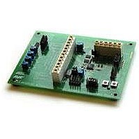
Fully Assembled Evaluation Board
Processor
ATmega406
Processor To Be Evaluated
ATmega406
Data Bus Width
8 bit
Interface Type
JTAG
For Use With/related Products
ATmega406
Lead Free Status / RoHS Status
Contains lead / RoHS non-compliant
Other names
Q2367281


2.1.5.1 Safety Signal
2.1.5.2 Charger Active Signal (BATT)
2.1.6 Test Points
2598C-AVR-06/06
Table 2-5. CONN1: Battery Pack Connections to Host or Charger
The PC0 I/O pin is used for the Safety Signal, as it is high-voltage compatible and is
also an output-only signal. The signal is impedance controlled. R26 provides a
permanent 10K resistance to ground so that whenever the pack is connected, the
Host or Charger sees a ‘Normal’ condition. When PC0 is driven low R22 provides a
1K resistance to GND, indicating a ‘Hot’ condition.
Additional I/O pins could be used, along with additional resistance values, to supply
all of the Safety Signal conditions indicated in the SMBus specification (see SMBus
spec. section 4.4.4 for more details).
When high voltage is present on the BATT pin and the AVR is in Power-Off mode, a
reset to occurs, thereby waking up a ‘sleeping’ pack when a charger is connected. A
diode is used to prevent internal battery voltage of the pack from being presented at
the pack’s external BATT terminal. BATT is also used to power the internal high-
voltage FET driver circuits for the Charge and Precharge FETs. Therefore the charger
must supply a voltage equal to B+ on the BATT signal. Note that since BATT is
connected via a diode as suggested, the FET pin drivers will only be able to bring the
gate to within a diode-drop of the BATT signal when turned off; the gate-source
resistors are left to further reduce the FET gate-source voltages to zero.
The SB100 board has several test points for development purposes. Figure 2-6
shows their placements on the board.
Figure 2-6. Test point placements
Pin
1
2
3
4
5
6
Name
B+
BATT
B-
SAFETY
SMBCLK
SMBDATA
Direction
I/O
Input
I/O
Output
I/O
I/O
Usage
Pack main positive high-current terminal
Charger Active signal
Pack main negative high-current terminal
Indicates pack safe/unsafe state
SMBus clock line
SMBus data line
AVR454
7
Related parts for ATAVRSB100
Image
Part Number
Description
Manufacturer
Datasheet
Request
R

Part Number:
Description:
DEV KIT FOR AVR/AVR32
Manufacturer:
Atmel
Datasheet:

Part Number:
Description:
INTERVAL AND WIPE/WASH WIPER CONTROL IC WITH DELAY
Manufacturer:
ATMEL Corporation
Datasheet:
Part Number:
Description:
Low-Voltage Voice-Switched IC for Hands-Free Operation
Manufacturer:
ATMEL Corporation
Datasheet:
Part Number:
Description:
MONOLITHIC INTEGRATED FEATUREPHONE CIRCUIT
Manufacturer:
ATMEL Corporation
Datasheet:
Part Number:
Description:
AM-FM Receiver IC U4255BM-M
Manufacturer:
ATMEL Corporation
Datasheet:
Part Number:
Description:
Monolithic Integrated Feature Phone Circuit
Manufacturer:
ATMEL Corporation
Datasheet:
Part Number:
Description:
Multistandard Video-IF and Quasi Parallel Sound Processing
Manufacturer:
ATMEL Corporation
Datasheet:
Part Number:
Description:
High-performance EE PLD
Manufacturer:
ATMEL Corporation
Datasheet:
Part Number:
Description:
8-bit Flash Microcontroller
Manufacturer:
ATMEL Corporation
Datasheet:
Part Number:
Description:
2-Wire Serial EEPROM
Manufacturer:
ATMEL Corporation
Datasheet: