ATAVRSB100 Atmel, ATAVRSB100 Datasheet - Page 10
ATAVRSB100
Manufacturer Part Number
ATAVRSB100
Description
SMART BATTERY DEVELOPMENT KIT
Manufacturer
Atmel
Type
Smart Batteryr
Datasheet
1.ATAVRSB100.pdf
(20 pages)
Specifications of ATAVRSB100
Contents
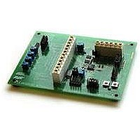
Fully Assembled Evaluation Board
Processor
ATmega406
Processor To Be Evaluated
ATmega406
Data Bus Width
8 bit
Interface Type
JTAG
For Use With/related Products
ATmega406
Lead Free Status / RoHS Status
Contains lead / RoHS non-compliant
Other names
Q2367281


2.3 Smart battery Circuit
2.3.1 Charging and discharging control
2.3.2 Precharge
2.3.3 Charge and discharge
10
AVR454
The ATmega406 provides a highly integrated solution that makes it easy to create an
SMBus compliant smart battery device with pack capacity monitoring with both
hardware and software safety features. Please see the device specification for more
details.
The FET transistors Q3 and Q4 provide the ability to disconnect the cells to prevent
accidental external short circuits from causing damage. Q5 provides separate control
over trickle charging, also referred to as pre-charging, used if the pack is over-
discharged, also known as a Deep Under-voltage condition.
Q5 and R27 control the Precharge circuit, whose purpose is to provide a mean to
supply charging current to an over-discharged pack whose voltage may be too low to
operate the ATmega406. The precharge current is limited by R27. R27 is sized so
that under maximum precharge current, its power dissipation does not create an
unsafe condition.
Generally the amount of precharge current required will depend on how quickly it is
desired to bring the cell stack up to a voltage level at which normal charging can
occur. This time depends in turn on the cell capacity. Assuming a 4-cell stack and a
worst-case discharge voltage of 0V (which should never be seen in practice!), the
applied charging voltage could be as high as
current to 10mA, a 1.68kΩ resistor would be required. The power dissipation of this
resistor would be 168mW, which would run rather hot (but not unsafely so) if
implemented as a 1206-size SMD component. However, given the fact that the cells
will likely never be as low as 0V, and assuming a more realistic figure such as 2.0V
for
precharge current requirements and number of cells in the stack would require
adjustments to this value and possibly to the physical size of the resistor.
Power MOSFET devices are present in virtually all Li-Ion battery packs to allow
completely disconnecting the cells from the outside world. This is necessary to
prevent intentional or accidental over-charge or over-discharge conditions as well as
short-circuits of the pack. This is accomplished by placing two FETs (Q3 and Q4)
back-to-back, allowing current flow to be stopped in both directions.
The ATmega406 provides active-low drive capability for external P-channel MOSFET
devices. If all three FETs are turned off, no current can flow in or out of the pack. If
either Q3 or Q4 is turned on, however, current will be allowed to flow in one direction,
namely through the internal body diode of the FET that is turned off. Thus, the
potential exists for overheating one or more FETs. Thus, the Discharge and Charge
FETs are always turned on and off together. Since the current through the Precharge
FET is limited, if that FET is on while the Discharge FET is off there will be very little
heat produced by the body diode of the Discharge FET.
The PVT pin is required to be connected to the high side of the battery stack to
perform its primary function, that of sensing Deep Under-voltage of the stack.
Additionally, this pin is the high-side power supply for the Discharge FET driver. This
arrangement creates a prerequisite that the Discharge FET to be placed closest to
(
16
8 .
V
an
−
4
⋅
2
0 .
over-discharged
V
)
2
/
1680
Ω
=
46
mW
cell,
, which is quite reasonable. Different
the
4
2 .
V
⋅
4
dissipation
=
16
8 .
V
. To limit precharge
would
2598C-AVR-06/06
be
Related parts for ATAVRSB100
Image
Part Number
Description
Manufacturer
Datasheet
Request
R

Part Number:
Description:
DEV KIT FOR AVR/AVR32
Manufacturer:
Atmel
Datasheet:

Part Number:
Description:
INTERVAL AND WIPE/WASH WIPER CONTROL IC WITH DELAY
Manufacturer:
ATMEL Corporation
Datasheet:
Part Number:
Description:
Low-Voltage Voice-Switched IC for Hands-Free Operation
Manufacturer:
ATMEL Corporation
Datasheet:
Part Number:
Description:
MONOLITHIC INTEGRATED FEATUREPHONE CIRCUIT
Manufacturer:
ATMEL Corporation
Datasheet:
Part Number:
Description:
AM-FM Receiver IC U4255BM-M
Manufacturer:
ATMEL Corporation
Datasheet:
Part Number:
Description:
Monolithic Integrated Feature Phone Circuit
Manufacturer:
ATMEL Corporation
Datasheet:
Part Number:
Description:
Multistandard Video-IF and Quasi Parallel Sound Processing
Manufacturer:
ATMEL Corporation
Datasheet:
Part Number:
Description:
High-performance EE PLD
Manufacturer:
ATMEL Corporation
Datasheet:
Part Number:
Description:
8-bit Flash Microcontroller
Manufacturer:
ATMEL Corporation
Datasheet:
Part Number:
Description:
2-Wire Serial EEPROM
Manufacturer:
ATMEL Corporation
Datasheet: